Semiconductor device and semiconductor memory device

a semiconductor memory and semiconductor technology, applied in semiconductor devices, digital storage, instruments, etc., can solve the problems of hindering the compactness of a semiconductor memory device, large number of defects in the vicinity of an interface between, etc., and achieve the effect of stabilizing the circuit operation

Active Publication Date: 2005-07-19
PANASONIC SEMICON SOLUTIONS CO LTD
View PDF4 Cites 212 Cited by
  • Summary
  • Abstract
  • Description
  • Claims
  • Application Information

AI Technical Summary

Benefits of technology

[0023]Therefore, an object of the present invention is to stabilize a circuit operation of a semiconductor device in which storage elements are arranged in an array and are surrounded by a large number of transistors regularly arranged, and to make such a semiconductor device compact.

Problems solved by technology

As such, when the adjacent diffusion layers are isolated through STI, a large stress occurs between an oxide film for isolation and the diffusion layers, thereby causing a large number of defects in the vicinity of an interface between the oxide film and the diffusion layers.
However, such occurrence of defects has not posed a significant problem in the conventional technology because a distance La from a gate electrode to an end of a diffusion layer shown in FIGS. 16 and 18 is relatively long.
This hinders a semiconductor memory device from being made compact.

Method used


Image

  • Semiconductor device and semiconductor memory device
  • Semiconductor device and semiconductor memory device
  • Semiconductor device and semiconductor memory device

Examples


Embodiment Construction

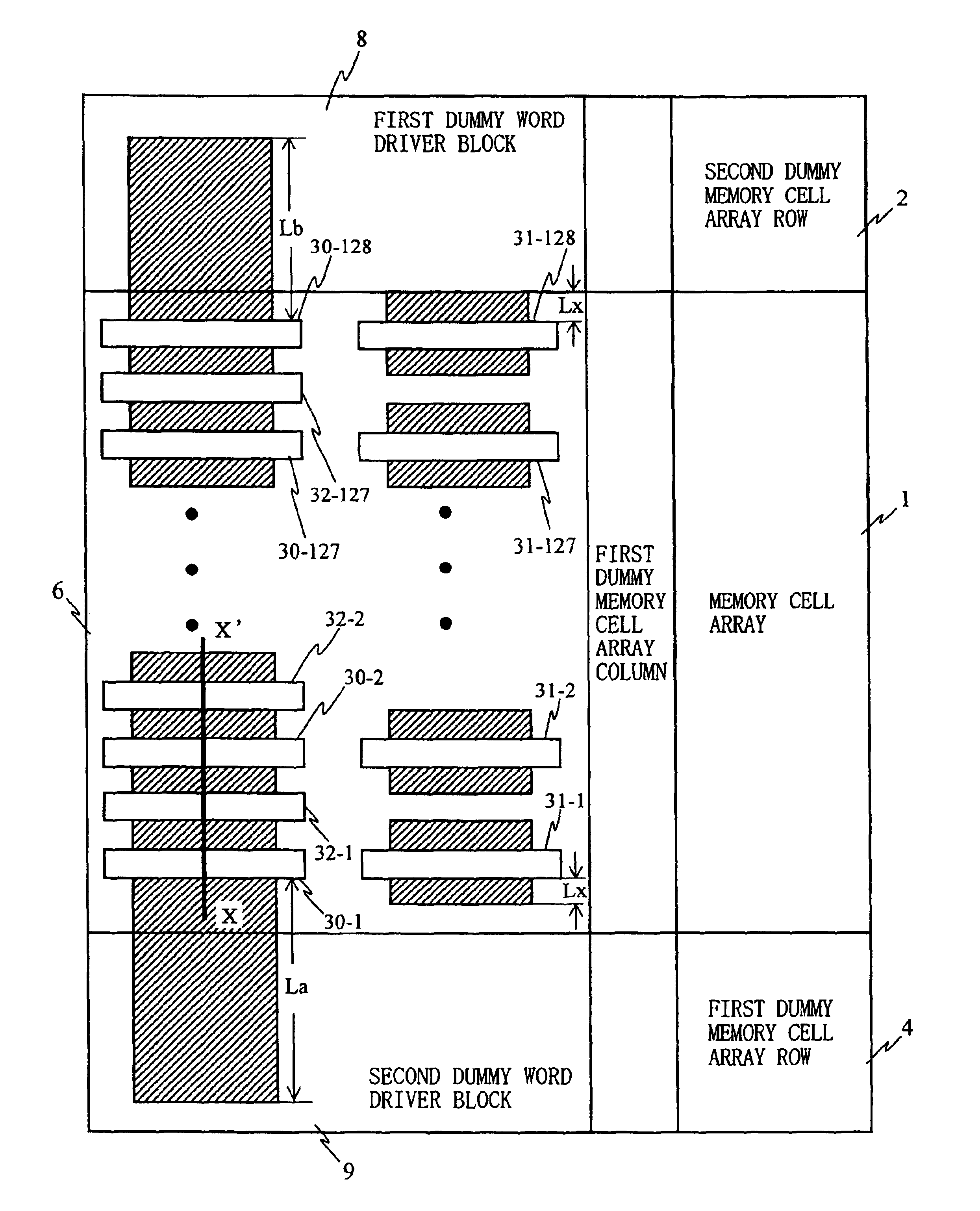
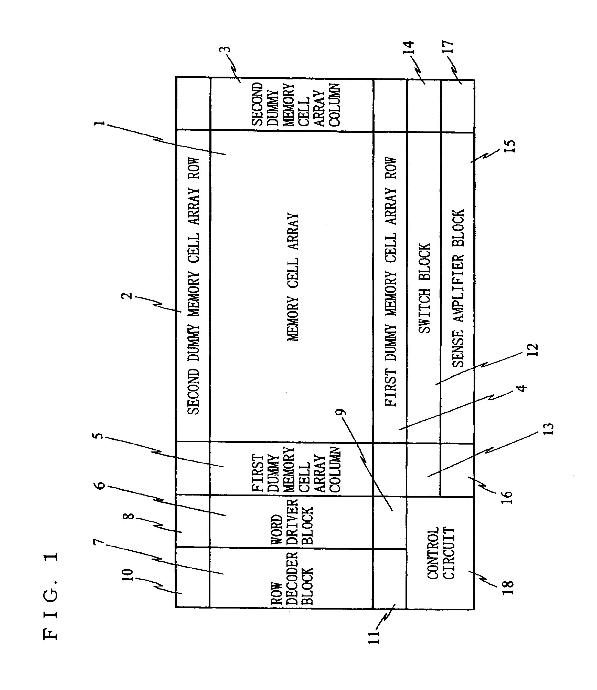
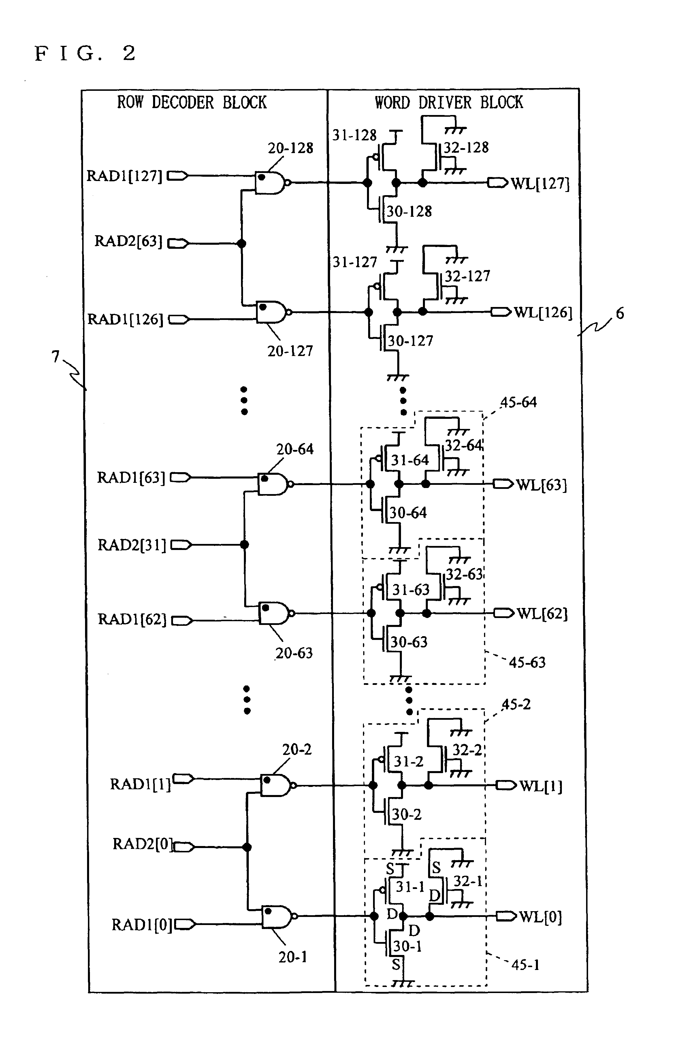
[0050]With reference to the drawings, a semiconductor memory device according to an embodiment of the present invention is described below. FIG. 1 is a block diagram showing the entire configuration of a semiconductor memory device according to the present embodiment. The semiconductor memory device shown in FIG. 1 is a 32-bit Static Random Access Memory (SRAM).

[0051]The semiconductor memory device shown in FIG. 1 includes a memory cell array 1, a second dummy memory cell array row 2, a second dummy memory cell array column 3, a first dummy memory cell array row 4, a first dummy memory cell array column 5, a word driver block 6, a row decoder block 7, a first dummy word driver block 8, a second dummy word driver block 9, a first dummy row decoder block 10, a second dummy row decoder block 11, a switch block 12, a first dummy switch block 13, a second dummy switch block 14, a sense amplifier block 15, a first dummy sense amplifier block 16, a second dummy sense amplifier block 17, an...


PUM


Abstract

A semiconductor memory device according to the present invention includes: a plurality of N-ch MOS transistors arranged in an area surrounding a plurality of memory cells arranged in an array, at a spacing depending on a spacing of the plurality of memory cells, for driving the plurality of memory cells; and a plurality of dummy transistors 32-j each of which is formed between two adjacent ones of the plurality of N-ch MOS transistors 30-k so as to share diffusion layers with adjacent N-ch MOS transistors 30 and each of which has a gate electrode supplied with a voltage for electrically insulating these adjacent transistors 30-k.

Description

BACKGROUND OF THE INVENTION[0001]1. Field of the Invention[0002]The present invention relates to a semiconductor device and, more specifically, a semiconductor device in which a plurality of elements identical in structure are arranged in an array.[0003]2. Description of the Background Art[0004]FIG. 13 is a block diagram showing the configuration of a conventional static random access memory (SRAM). With reference to FIG. 13, the conventional SRAM is described.[0005]The SRAM shown in FIG. 13 includes a memory cell array 1001, a second dummy memory cell array row 1002, a second dummy memory cell array column 1003, a first dummy memory cell array row 1004, a first dummy memory cell array column 1005, a word driver block 1006, a row decoder block 1007, a switch block 1012, and a sense amplifier block 1015.[0006]The memory cell array 1001, the second dummy memory cell array row 1002, the second dummy memory cell array column 1003, the first dummy memory cell array row 1004, and the firs...

Claims


Application Information

Patent Timeline
Patent Type & Authority Patents(United States)
IPC IPC(8): G11C11/412H01L27/11G11C11/41H01L21/8244
CPCG11C11/412H01L27/11H10B10/00
Inventor SHIBAYAMA, AKINORI
Owner PANASONIC SEMICON SOLUTIONS CO LTD
Why Eureka
Try Eureka