Methods for generating output control signals in synchronous semiconductor memory devices and related semiconductor memory devices

a technology of output control and synchronous semiconductor memory, which is applied in the direction of static storage, digital storage, instruments, etc., can solve the problem of negatively affecting the speed of operation of synchronous semiconductor memory devices

Active Publication Date: 2005-07-19
SAMSUNG ELECTRONICS CO LTD
View PDF2 Cites 23 Cited by
  • Summary
  • Abstract
  • Description
  • Claims
  • Application Information

AI Technical Summary

Problems solved by technology

Accordingly, clock jitter in the external clock signal may act to reduce the available timing margin which negatively impacts the speed of operation of the synchronous semiconductor memory device.

Method used


Image

  • Methods for generating output control signals in synchronous semiconductor memory devices and related semiconductor memory devices
  • Methods for generating output control signals in synchronous semiconductor memory devices and related semiconductor memory devices
  • Methods for generating output control signals in synchronous semiconductor memory devices and related semiconductor memory devices

Examples


Embodiment Construction

[0029]The present invention will now be described more fully with reference to the accompanying drawings, in which typical embodiments of the invention are shown. This invention, however, may be embodied in many different forms and should not be construed as limited to the embodiments set forth herein. Rather, these embodiments are provided so that this disclosure will be thorough and complete, and will fully convey the scope of the invention to those skilled in the art. It will also be understood that when an element is referred to as being “coupled” or “connected” to another element that it can be directly coupled or connected to the other element or that intervening elements may also be present. In contrast, when an element is referred to as being “directly coupled” or “directly connected” to another element, there are no intervening elements present. Like reference numerals refer to like elements throughout this application.

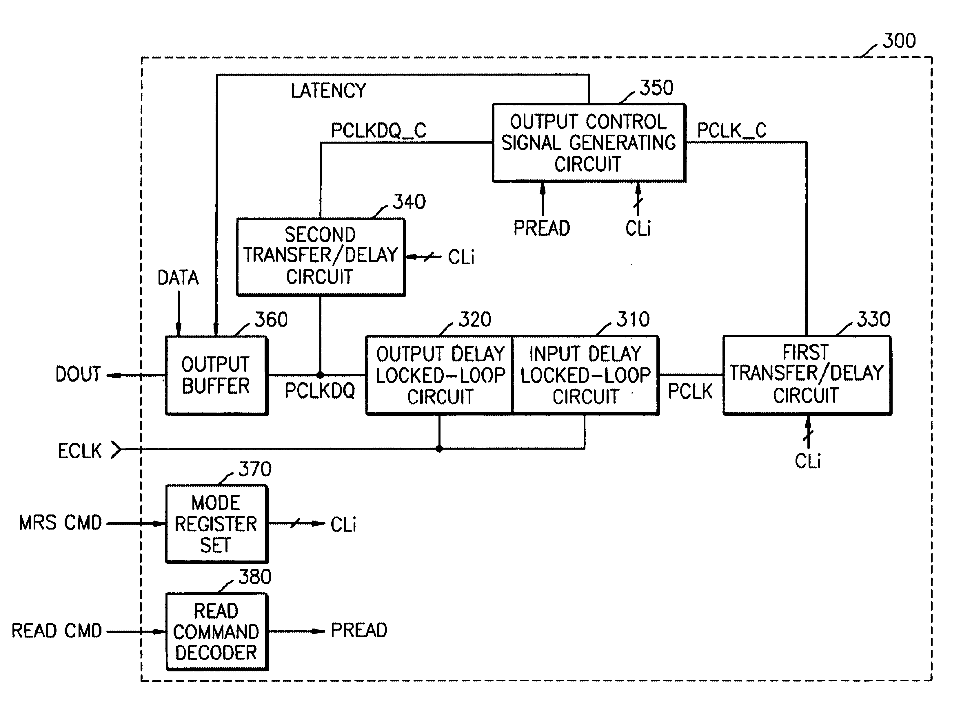
[0030]FIG. 3 is a block diagram of a synchronous semico...


PUM


Abstract

A synchronous semiconductor memory device includes an output control signal generating circuit that generates a data output control signal in response to an internal clock signal, an output control clock signal and a CAS latency signal. The output control signal generating circuit successively shifts read information signals in response to the internal clock signal and the output control clock signal, both source clocks of which are identical, and generates one of the shifted read information signals as an output control signal for indicating a data output period in response to the CAS latency signal. The synchronous semiconductor memory device can synchronize the source clocks of the clock signals used in the output control signal generating circuit thereby reducing the influence of clock jitter.

Description

RELATED APPLICATION[0001]This application claims the priority of Korean Patent Application No. 2002-78386 filed on Dec. 10, 2002, in the Korean Intellectual Property Office, the disclosure of which is incorporated herein in its entirety by reference.FIEL OF THE INVENTION[0002]The present invention relates to semiconductor memory devices, and more particularly, to methods for generating output control signals in synchronous semiconductor memory devices and related synchronous semiconductor memory devices.DESCRIPTION OF THE RELATED ART[0003]Semiconductor memory devices are used as the primary memory storage device in many computer systems. The rate at which data may be input to or output from a semiconductor memory device may be an important factor in determining the operating speed of the computer system. To improve operating speeds of semiconductor memory devices, synchronous dynamic random access memory (SDRAM) devices have been used in which the memory device operates in synchroni...

Claims


Application Information

Patent Timeline
Patent Type & Authority Patents(United States)
IPC IPC(8): G11C7/00G11C7/10G11C7/22G11C11/4076G11C11/407G11C11/40G11C11/409
CPCG11C7/1072G11C7/22G11C7/222G11C11/4076G11C11/40
Inventor CHUNG, DAE-HYUNSHIN, SANG-WOONG
Owner SAMSUNG ELECTRONICS CO LTD
Why Eureka
Try Eureka