Method and apparatus for characterization of devices and circuits

a technology of devices and circuits, applied in the direction of instruments, material heat development, heat measurement, etc., can solve the problems of inadequacies in device parameters determination, affecting the performance of optical systems using semiconductor lasers as light sources, and affecting the performance of optical systems using semiconductor lasers

Inactive Publication Date: 2005-07-26
MASSACHUSETTS INST OF TECH
View PDF17 Cites 35 Cited by
  • Summary
  • Abstract
  • Description
  • Claims
  • Application Information

AI Technical Summary

Problems solved by technology

For example, optical systems which utilize semiconductor lasers as light sources can lose performance due to heating of the laser at high power levels and the consequent well-known phenomenon of efficiency rollover.
These methods can be hampered in situations where such detectors are not available (as is true for certain wavelengths of light) or are not able to be positioned in the path of the light.
Additional complications with calibration arise when optical systems employ devices at many different wavelengths.
Since this prior method relies on an optical detector, this prior method is inapplicable in the case of integrated photonic systems, and also is not appropriate for the determination of device parameters over a range of bias.

Method used


Image

  • Method and apparatus for characterization of devices and circuits
  • Method and apparatus for characterization of devices and circuits
  • Method and apparatus for characterization of devices and circuits

Examples


Embodiment Construction

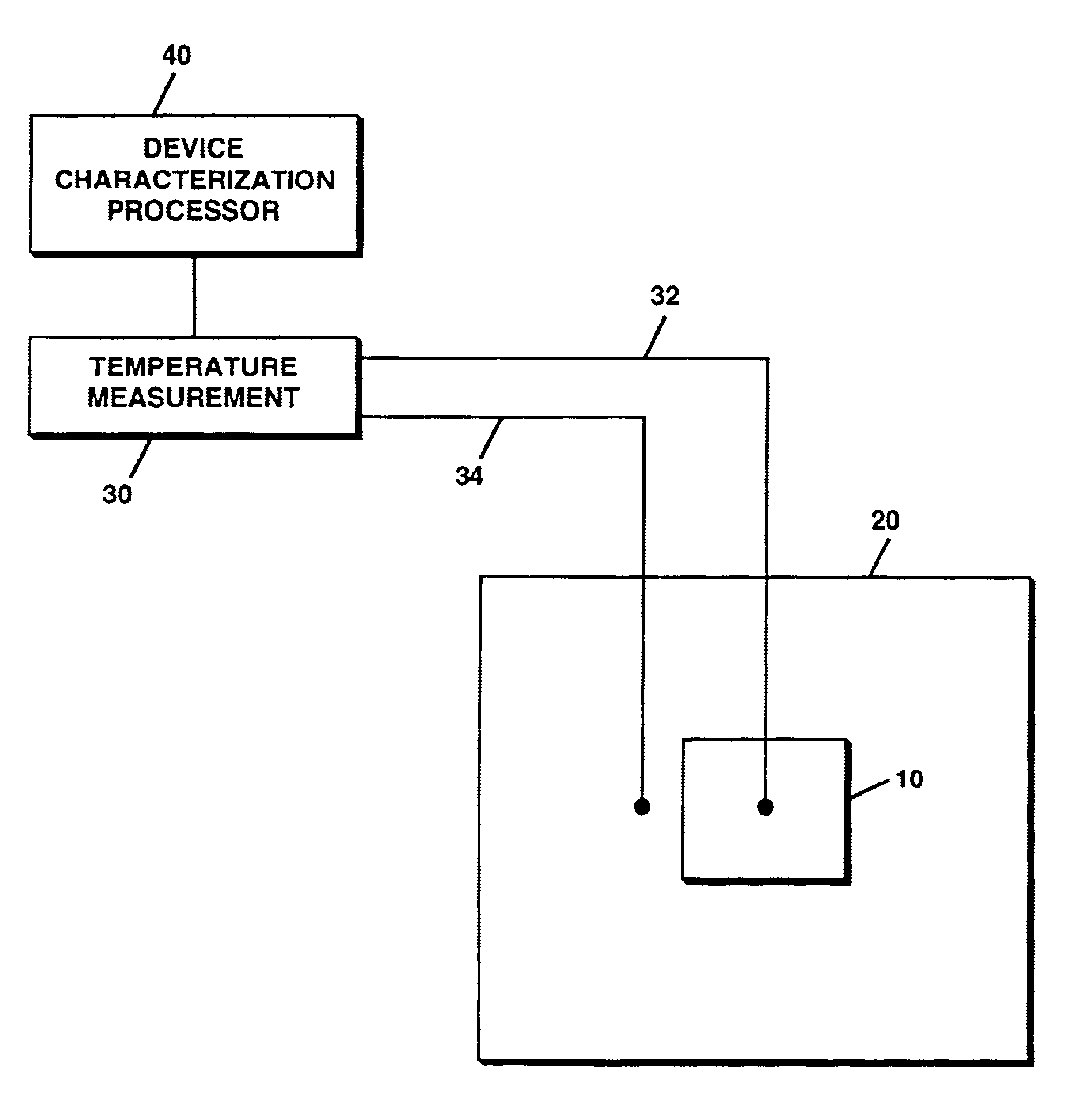
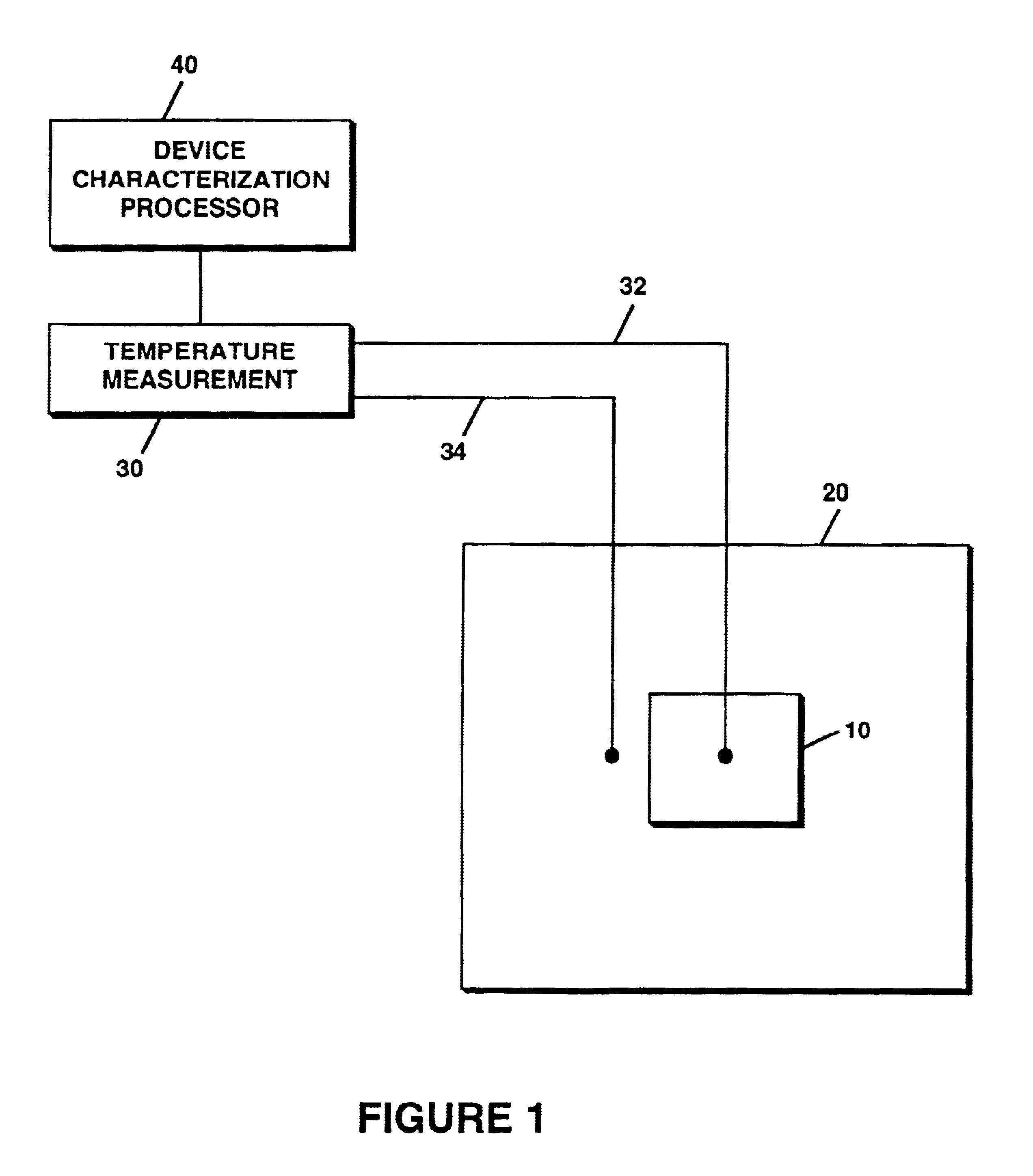
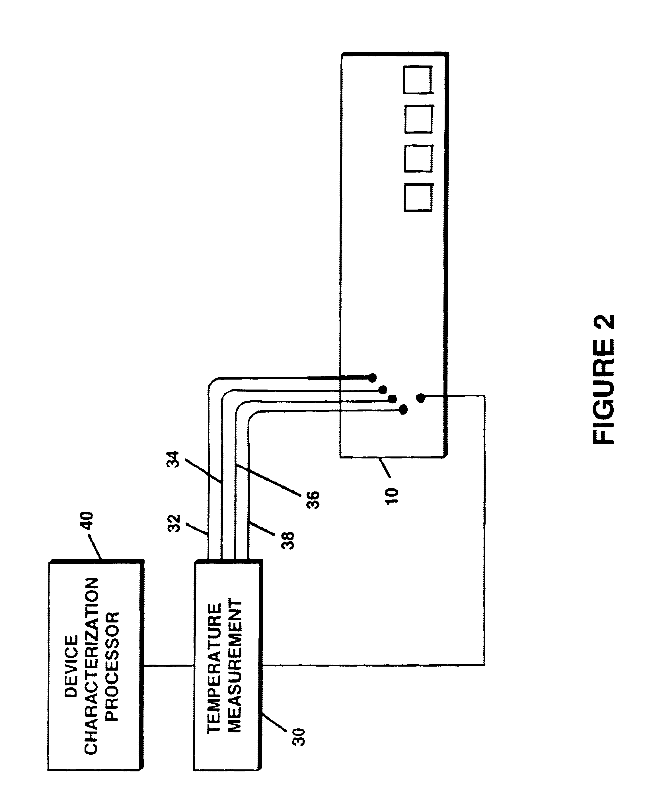
[0018]A method and apparatus for characterization of photonic devices and circuits is presented. A thermal sensor is used to measure an internal or a surface temperature of a device. The sensor is then moved (or a second sensor is used) to measure a temperature in a second location. Alternately a reference temperature may be used. The difference between the two temperatures is determined. The temperatures and / or the temperature difference are related mathematically to characteristics (for example, the power being dissipated) of the device. Device characteristics are then derived by mathematical means. The device characteristics may include, but are not limited to, optical power, power dissipation, radiated power, spontaneous emission power, electron temperature, optical absorption, optical gain, heat transfer coefficient, threshold current, spontaneous emission efficiency, stimulated emission efficiency and thermal impedance.

[0019]The invention described herein uses a thermal sensor...


PUM

PropertyMeasurementUnit
temperatureaaaaaaaaaa
series resistanceaaaaaaaaaa
thicknessaaaaaaaaaa

Abstract

A method and apparatus for performing characterization of devices is presented. The characteristic of the device are determined by obtaining a first temperature measurement in a first location of a device, obtaining a second temperature measurement, computing the difference between the temperature measurements and, using the temperatures and/or the temperature difference, a characteristic of the device is determined.

Description

CROSS REFERENCE TO RELATED APPLICATIONS[0001]This application claims priority under 35 U.S.C. § 119(e) to provisional patent application Ser. No. 60 / 356,492 filed Feb. 12, 2002; the disclosure of which is incorporated by reference herein.STATEMENT REGARDING FEDERALLY SPONSORED RESEARCH[0002]This invention was made with government support under Grant Number BX-7556 awarded by the U.S. Air Force. The government has certain rights in the invention.BACKGROUND OF THE INVENTION[0003]The reliable functioning of optical components is of critical importance in optical systems, which typically have small tolerances. Parameters such as device efficiency (which describes the amount of conversion between electrical and optical energy) govern the performance of an optical system. For example, optical systems which utilize semiconductor lasers as light sources can lose performance due to heating of the laser at high power levels and the consequent well-known phenomenon of efficiency rollover.[0004...

Claims


Application Information

Patent Timeline
Patent Type & Authority Patents(United States)
IPC IPC(8): G01K3/00G01N25/18
CPCG01K3/00G01N25/18
Inventor PIPE, KEVIN P.RAM, RAJEEV J.
Owner MASSACHUSETTS INST OF TECH
Why Eureka
Try Eureka