Ball grid array package

a grid array and package technology, applied in the field of ball grid array (bga) package, can solve the problems of difficulty and risks of wire bonding, the pitch of the bond pad on the semiconductor die is typically restricted from achieving a comparable pitch, and the speed and complexity of ic chip increase, so as to improve the arrangement of the bonding pad and reduce the difficulty of wire bonding. , the effect of increasing the tier of the bonding wir

Inactive Publication Date: 2005-07-26
ADVANCED SEMICON ENG INC
View PDF6 Cites 14 Cited by
  • Summary
  • Abstract
  • Description
  • Claims
  • Application Information

AI Technical Summary

Benefits of technology

[0014]Therefore, only three tiers of bonding wires with different loop heights are required for avoiding short circuiting wherein the bonding wires electrically connect the chip to the substrate. The lower tier bonding wires connect the ground pads / power supply pads designed in the outer row of the bonding pads to the ground ring / power ring of the substrate, and connect the I / O pads of the outer row to the corresponding conductive traces on the substrate. The middle tier bonding wires connect the I / O pads designed in the middle row of the bonding pads to corresponding conductive traces of the substrate. The upper tier bonding wires connect the I / O pads designed in the inner row of the bonding pads to corresponding conductive traces of the substrate. Therefore, the three tiers of bonding wires only require three times of wire bonding operation.
[0015]As mentioned above, the BGA package according to the present invention has a better arrangement of the bonding pads so as to meet the requirement of the chip with high I / O pads without increasing tiers of the bonding wires, thereby decreasing the difficulty of wire bonding. In addition, increasing the maximum allowable pad number has the benefit of providing not only more bonding pads per chip but also shorter metal wires and thus faster circuits.

Problems solved by technology

As electronic devices have become more smaller and thinner, the velocity and the complexity of IC chip become more and more higher.
Although the conductive traces pads on a BGA substrate can be lithographically defined to achieve a very fine pitch, the bond pad pitch on the semiconductor die is typically restricted from achieving a comparable pitch due to spacing and design rules used to account for wire bonding methods and tolerances, such as capillary tool interference during wire bonding.
Difficulty and risks of wire bonding are proportional to the times of wire bonding operation required.
However, the patent also failed to provide a proper arrangement of the bonding pads to meet the requirement of the chip with high I / O pads.

Method used


Image

  • Ball grid array package
  • Ball grid array package
  • Ball grid array package

Examples


first embodiment

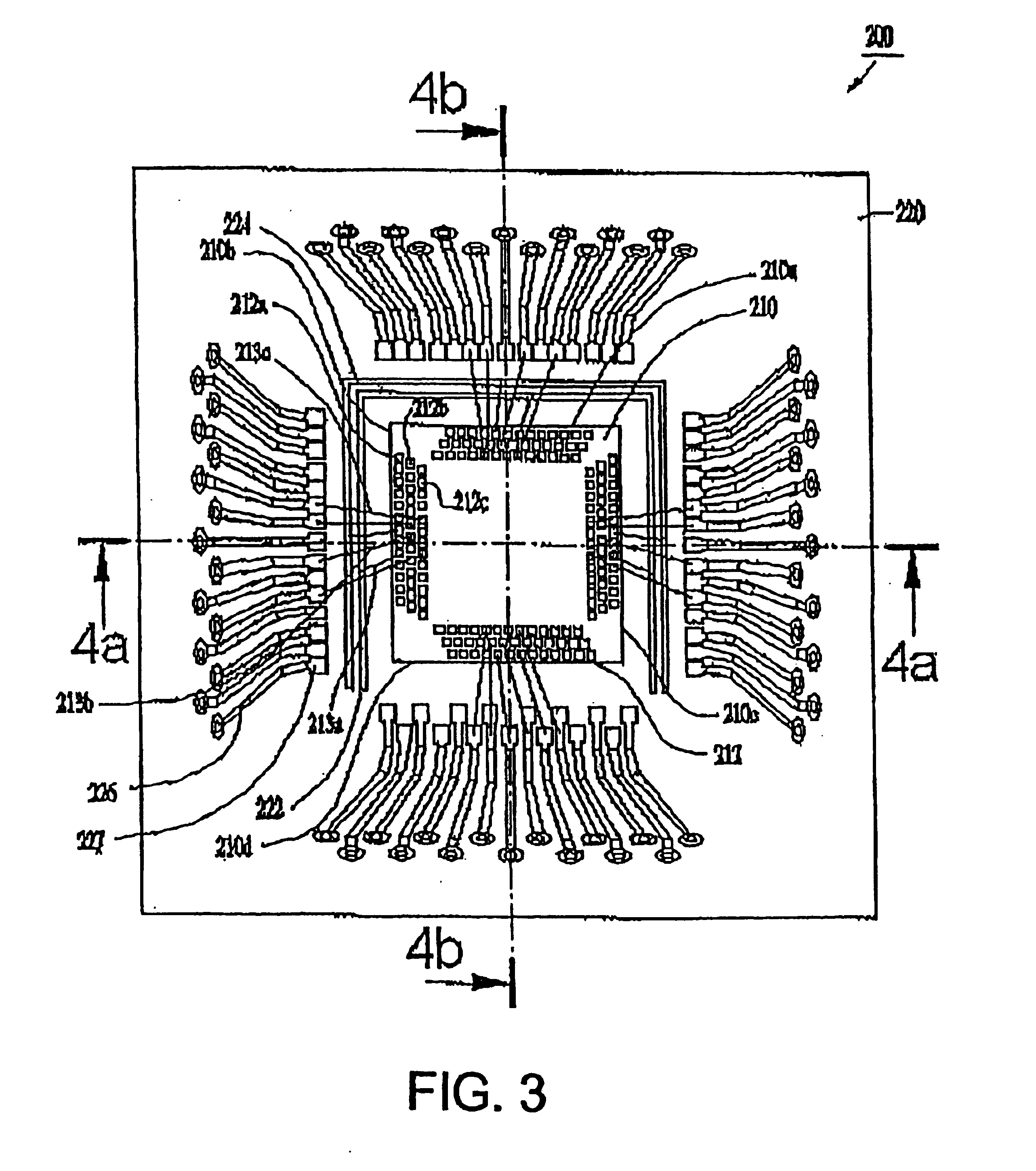
[0022]FIG. 3 depicts a schematic top plan view of a BGA package 200 according to the present invention. The BGA package 200 comprises a chip 210 with an array pad design having a substantially square shape disposed on the top surface of a substrate 220. The chip 210 and the top surface of the substrate 220 are encapsulated in a package body 230 (shown in FIG. 4).

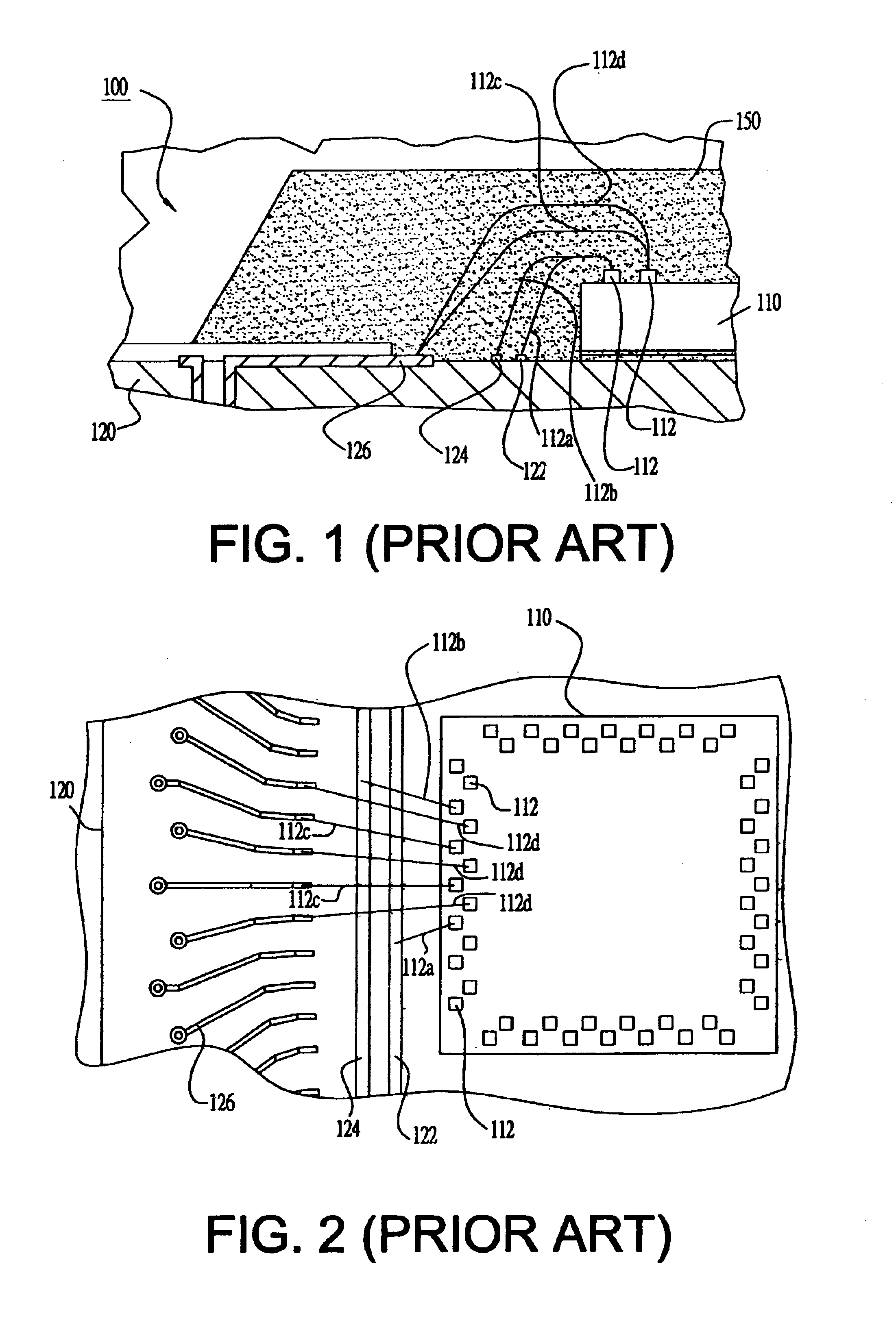
[0023]Referring to FIG. 4, the top surface of the substrate 220 is provided with a ground ring 222, a power ring 224, and a plurality of conductive traces 226 with fingers 227 arranged at the periphery of the ground ring 222 and the power ring 224. The bottom surface of the substrate 220 is provided with a plurality of solder pads (not shown) electrically connected to the ground ring 222, the power ring 224, and the conductive traces 226, respectively. Each of the solder pads is provided with a solder ball for making external electrical connection. The chip 210 has a plurality of bonding pads 212 formed on the active surface...

second embodiment

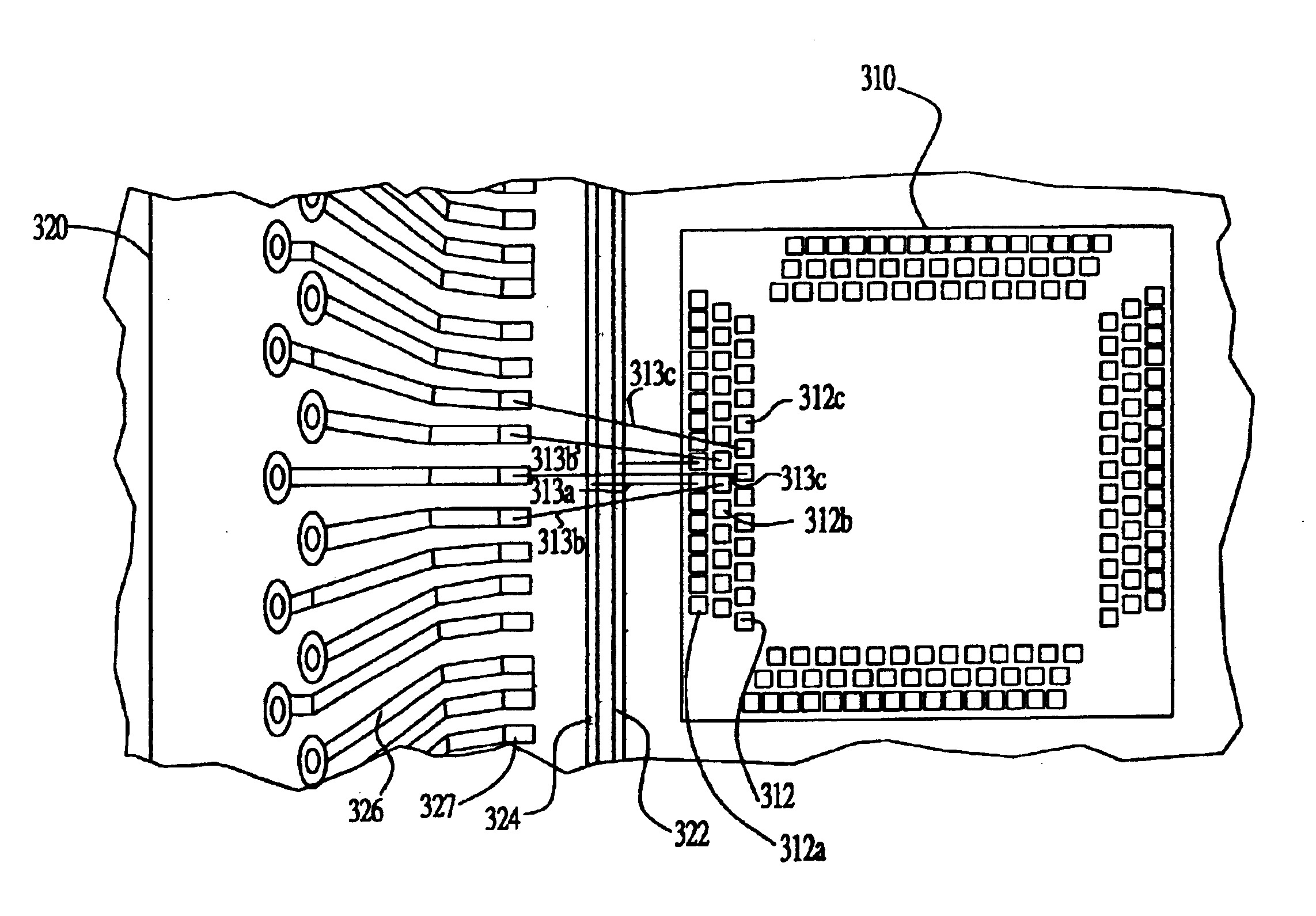
[0027]FIG. 5 discloses a partial top plan view of a BGA package with the package body being removed according to the present invention. The BGA package 300 is substantially identical to the BGA package 200 of FIG. 4 with the exceptions that the bond pad pitch of the outer row 312a of the bonding pads 312 is smaller than that of the middle row 312b and the inner row 312c of the bonding pads 312 on chip 310, and each bonding wire 313a of the lower tier is bonded to be substantially vertical to the corresponding edge of the chip 310. Since the lower tier bonding wires 313a connected to the outer row 312a of the bonding pads are substantially vertical to the corresponding edge of the chip 310, there is no need to consider the horizontal wire pitch arrangement between the lower tier bonding wires 313a. Therefore, the bond pad pitch of the outer row 312a of the bonding pads can be designed to be smaller than that of the middle row 312b and the inner row 312c of the bonding pads on chip 31...


PUM


Abstract

A BGA package comprises a chip with an array pad design disposed on the top surface of a substrate. The chip has a plurality of bonding pads located about the periphery thereof. The bonding pads of the chip are positioned in three rows, an inner row, a middle row, and an outer row along the sides of the chip. All of the power supply pads and ground pads are adjacent to one another and designed in the outer row of the bonding pads, and the I/O pads are designed in the outer row, the middle row and the inner row of the bonding pads. The outer row, middle row, and the inner row of the bonding pads are electrically connected to the substrate through three tiers of bonding wires with different loop height, respectively.

Description

BACKGROUND OF THE INVENTION[0001]1. Field of the Invention[0002]This invention generally relates to a ball grid array (BGA) package, and more particularly to a BGA package using wire-bonding technique.[0003]2. Description of the Related Art[0004]As electronic devices have become more smaller and thinner, the velocity and the complexity of IC chip become more and more higher. Accordingly, a need has arisen for higher package efficiency. To meet the need, the ball grid array (BGA) technology has been developed by the semiconductor industry.[0005]Although the conductive traces pads on a BGA substrate can be lithographically defined to achieve a very fine pitch, the bond pad pitch on the semiconductor die is typically restricted from achieving a comparable pitch due to spacing and design rules used to account for wire bonding methods and tolerances, such as capillary tool interference during wire bonding.[0006]Conventional IC bond pad designs include (a) single in-line bond pad design a...

Claims


Application Information

Patent Timeline
Patent Type & Authority Patents(United States)
IPC IPC(8): H01L23/498H01L23/48
CPCH01L23/49838H01L24/06H01L24/49H01L2224/04042H01L2224/05599H01L2224/48095H01L2224/49171H01L2224/49175H01L2224/49431H01L2224/85399H01L2924/01005H01L2924/01006H01L2924/014H01L2924/14H01L2924/00014H01L24/48H01L2924/01033H01L2224/32225H01L2224/73265H01L2924/00H01L2224/48227H01L2224/45099H01L2224/05554H01L2224/023H01L2924/181H01L2924/00012H01L2924/0001
Inventor TIEN, YUN HSIANG
Owner ADVANCED SEMICON ENG INC
Why Eureka
Try Eureka