Area efficient charge pump

a charge pump and efficient technology, applied in the field of voltage generation circuits, can solve the problems of large capacitor area, difficulty in providing additional oxides, and high cost, and achieve the effect of reducing the dielectric of the thinner capacitor and reducing the area

Inactive Publication Date: 2005-07-26
SANDISK TECH LLC
View PDF12 Cites 123 Cited by
  • Summary
  • Abstract
  • Description
  • Claims
  • Application Information

AI Technical Summary

Benefits of technology

[0011]The following description and figures disclose other aspects and advantages of the present invention.

Problems solved by technology

Unfortunately it is very difficult and / or costly to provide additional oxides whose thickness can be optimized for any specific multiple of VCC.
The disclosed implementation includes one capacitor per stage, but like that shown in U.S. Pat. No. 5,436,587 referenced earlier, the capacitor must be capable of sustaining a progressively higher voltage at each stage, and thus suffers the same disadvantage of large capacitor area.

Method used


Image

  • Area efficient charge pump
  • Area efficient charge pump
  • Area efficient charge pump

Examples


Embodiment Construction

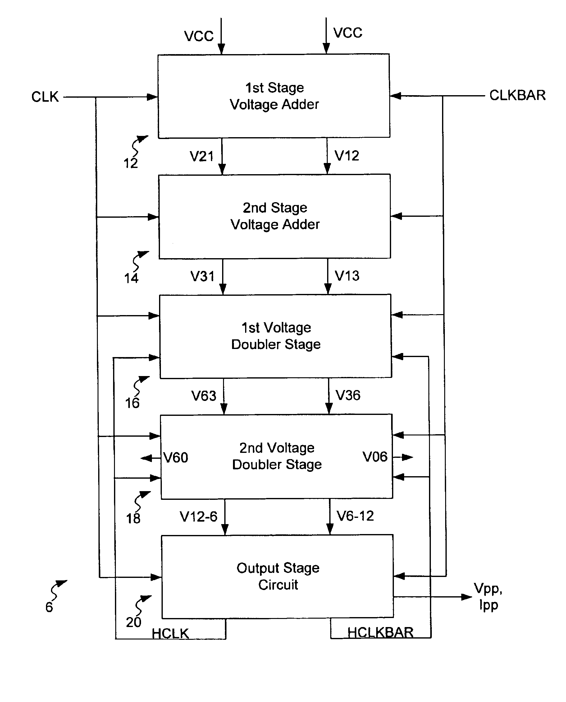
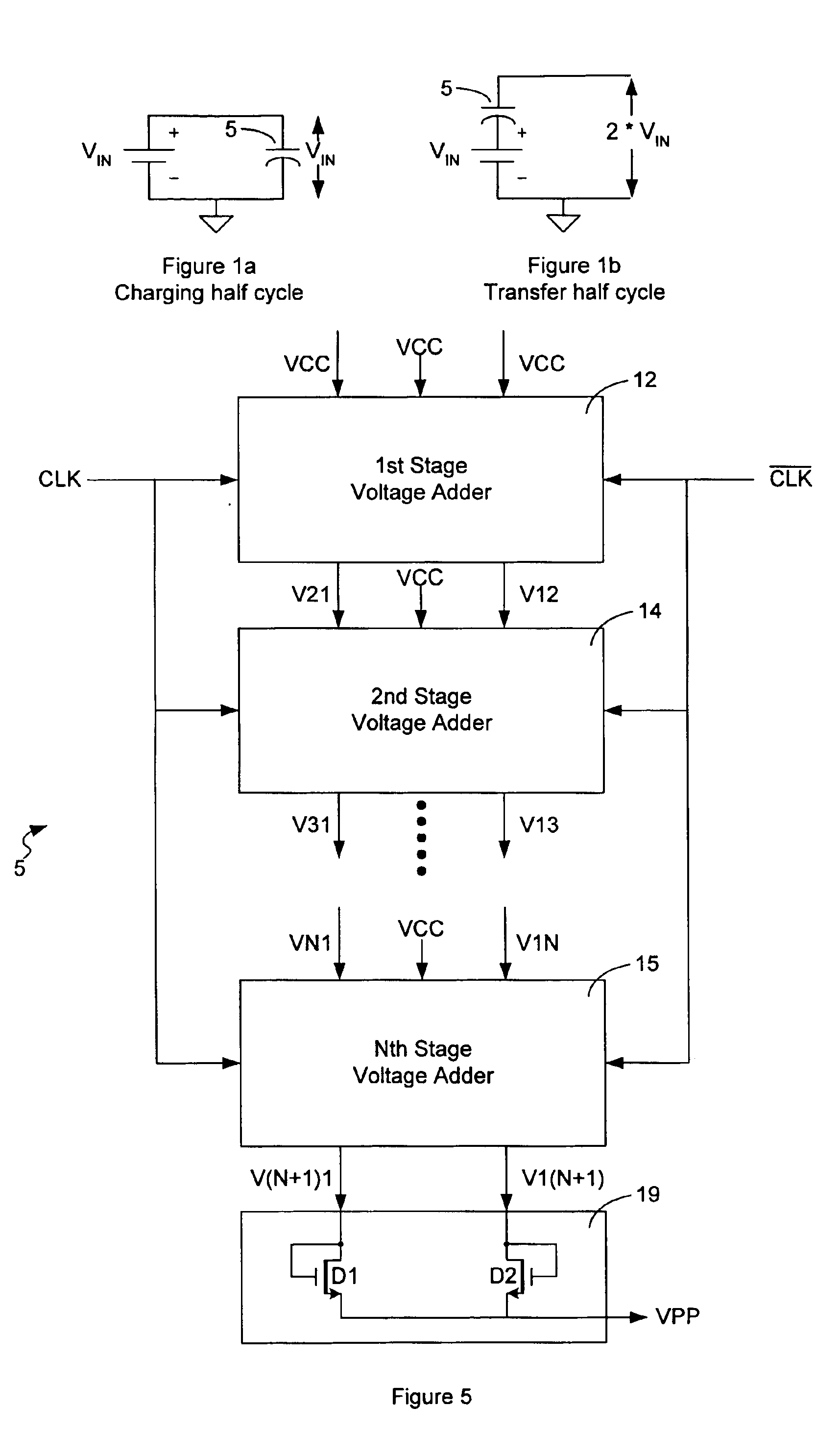
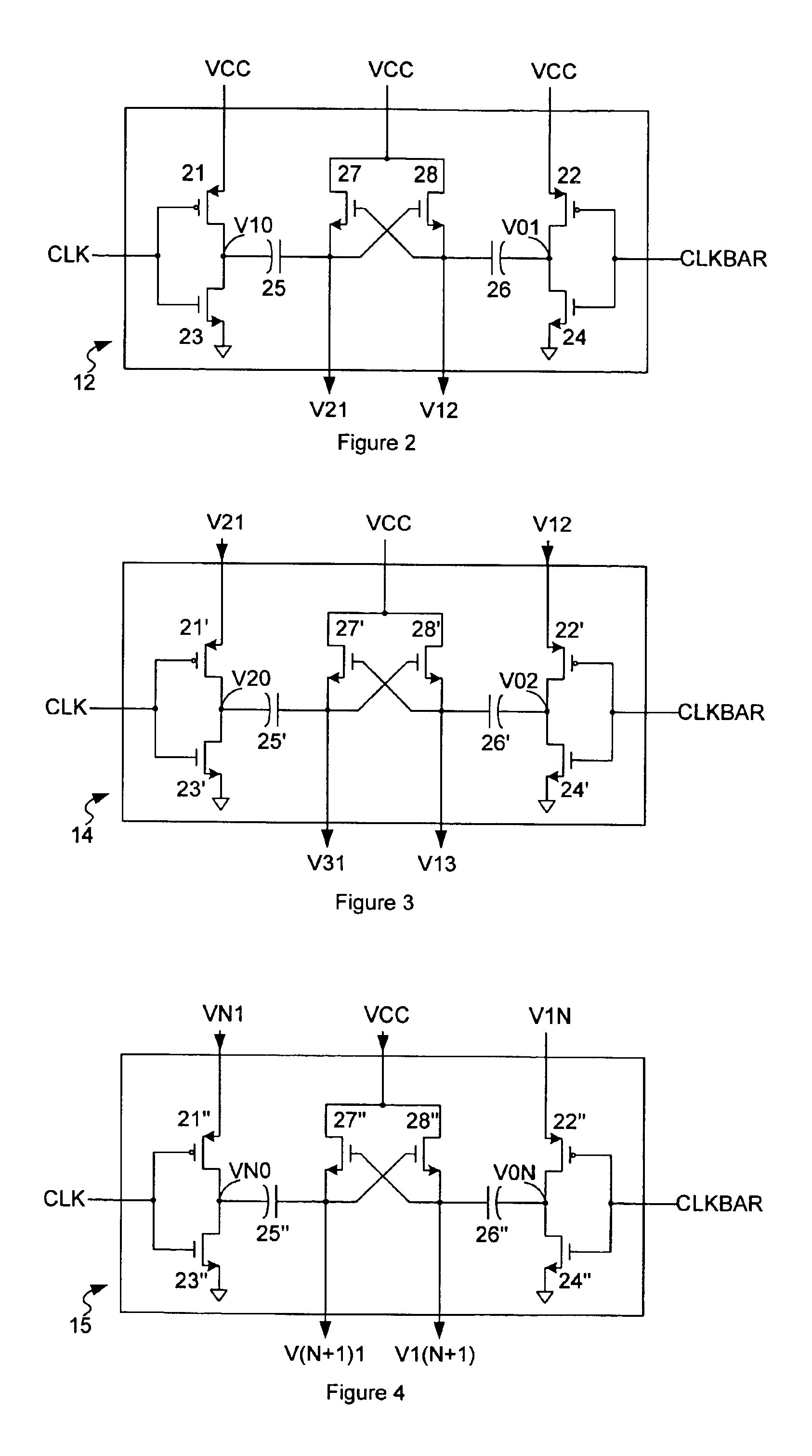
[0025]In FIG. 2, a circuit diagram for a first voltage adder stage 12 is illustrated. Two signals, CLK and its complement, CLKBAR, are inputs to this stage. These signals alternate between voltage levels VCC and ground at approximately a 50% duty cycle, such that when CLK is low, CLKBAR is high and when CLK is high, CLKBAR is low. In the description that follows, the voltage level of CLK will be defined as low (ground) during odd numbered half cycles, and high (VCC) during even numbered half cycles. For ease of explanation we will assume that the desired charge pump output voltage is positive with respect to a ground reference and that VCC is a more positive voltage than ground, but the techniques described are equally applicable to producing negative voltage charge pumps by suitable change of the reference level. As will be explained shortly, the name used to identify each voltage variable node, Vij with i and j as integers, is chosen to not only identify a unique node name but als...


PUM


Abstract

A first charge pump includes a collection of voltage adder stages. The first voltage adder stage receives an input voltage VCC and in response to a clock signal provides a first voltage signal alternating between 2*VCC and VCC. The Nth voltage adder stage receives an input voltage VCC and a first voltage signal from the preceding stage, and provides a second voltage signal alternating between N*VCC and VCC. The capacitors included within each adder stage are required to sustain a maximum voltage of VCC. In an alternate embodiment the first charge pump may be combined with one or more voltage doubler stages to produce even higher output voltages.

Description

FIELD OF THE INVENTION[0001]This invention pertains generally to voltage generation circuits and more particularly to a charge pump circuit that is area efficient when implemented in applications such as an integrated circuit.BACKGROUND OF THE INVENTION[0002]Charge pumps use a switching process to provide a DC output voltage larger than its DC input voltage. In general, a charge pump will have a capacitor coupled to switches between an input and an output. During one clock phase, the charging half cycle, the capacitor couples in parallel to the input so as to charge up to the input voltage. During a second clock phase, the transfer half cycle, the charged capacitor couples in series with the input voltage so as to provide an output voltage twice the level of the input voltage. This process is illustrated in FIGS. 1a and 1b. In FIG. 1a, the capacitor 5 is arranged in parallel with the input voltage VIN to illustrate the charging half cycle. In FIG. 1b, the charged capacitor 5 is arra...

Claims


Application Information

Patent Timeline
Patent Type & Authority Patents(United States)
IPC IPC(8): G05F3/02G05F1/10G11C5/14H02M3/07H02M3/04
CPCG11C5/145H02M3/073H02M3/07G11C5/14
Inventor CERNEA, RAUL-ADRIAN
Owner SANDISK TECH LLC
Why Eureka
Try Eureka