Strained silicon layer semiconductor product employing strained insulator layer

a technology semiconductor products, applied in the direction of semiconductor devices, electrical appliances, basic electric elements, etc., can solve the problems of not entirely without problems, and it is difficult in the fabrication art of strained silicon layer structures to efficiently fabricate them, so as to enhance fabrication efficiency and enhance fabrication efficiency

Inactive Publication Date: 2005-08-02
TAIWAN SEMICON MFG CO LTD
View PDF8 Cites 40 Cited by
  • Summary
  • Abstract
  • Description
  • Claims
  • Application Information

AI Technical Summary

Benefits of technology

[0018]The present invention provides a strained silicon layer structure for use within a semiconductor product, wherein the strained silicon layer structure has enhanced fabrication efficiency.
[0019]The present invention realizes the foregoing object by employing within a strained silicon layer structure within a strained silicon layer fabrication a strained insulator material layer formed over a strained silicon lay

Problems solved by technology

While strained silicon materials and structures are thus desirable in the semiconductor product fabrication art, they are nonetheless not entirely without problems.
In that regard, it is often difficult in the semiconductor pr

Method used


Image

  • Strained silicon layer semiconductor product employing strained insulator layer
  • Strained silicon layer semiconductor product employing strained insulator layer

Examples


Embodiment Construction

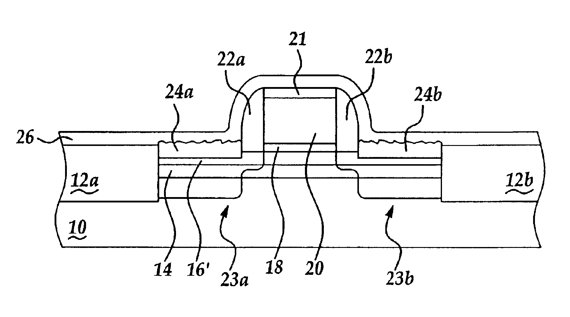
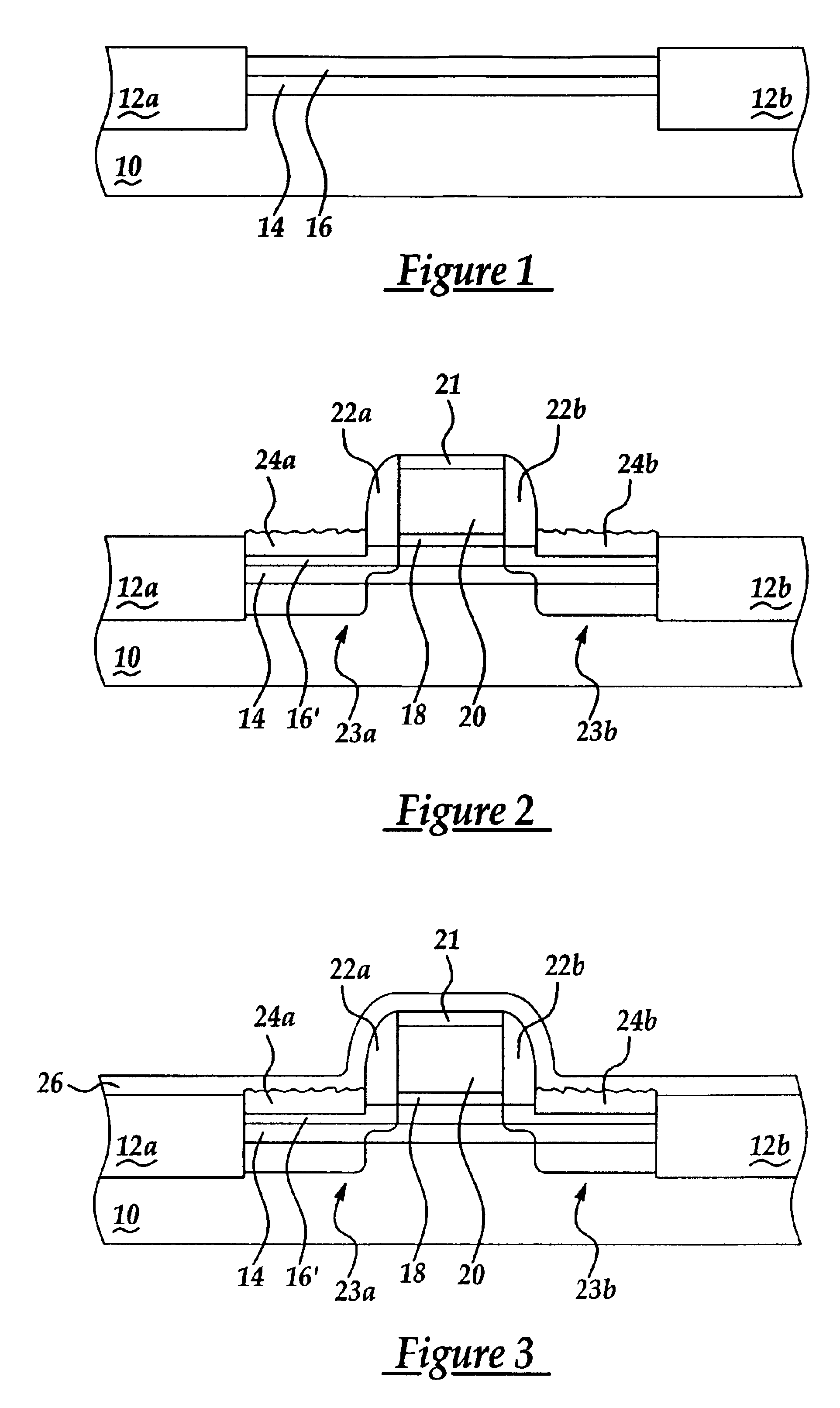
[0022]The present invention provides a strained silicon layer structure for use within a semiconductor product, wherein the strained silicon layer structure has enhanced fabrication efficiency.

[0023]The present invention realizes the foregoing object by employing within a strained silicon layer structure within a strained silicon layer fabrication a strained insulator material layer formed over a strained silicon layer in turn formed upon a strained silicon-germanium alloy material layer which is formed upon a relaxed material substrate. Within the invention, the strained insulator material layer provides additional fabrication options when fabricating the strained silicon layer structure within the strained silicon layer fabrication. Thus the strained silicon layer structure may be fabricated with enhanced fabrication efficiency.

[0024]While the preferred embodiment of the invention illustrates the invention most specifically within the context of a field effect transistor device fo...


PUM


Abstract

A strained silicon layer fabrication and a method for fabrication thereof employ a strained insulator material layer formed over a strained silicon layer in turn formed upon a strained silicon-germanium alloy material layer which is formed upon a relaxed material substrate. The strained insulator material layer provides increased fabrication options which provide for enhanced fabrication efficiency when fabricating the strained silicon layer fabrication.

Description

BACKGROUND OF THE INVENTION[0001]1. Field of the Invention[0002]The present invention relates generally to strained silicon layer structures employed within semiconductor products. More particularly, the present invention relates to enhanced fabrication efficiency strained silicon layer structures employed within semiconductor products.[0003]2. Description of the Related Art[0004]As semiconductor product performance requirements have increased, so also have evolved novel semiconductor materials and structures which provide enhanced semiconductor product performance. Included among such novel materials and structures are strained silicon materials and structures which may be employed as substrates when forming semiconductor devices. Strained silicon materials and structures are desirable as semiconductor substrates insofar as strained silicon materials provide for enhanced carrier mobility and thus enhanced performance of semiconductor devices.[0005]While strained silicon materials a...

Claims


Application Information

Patent Timeline
IPC IPC(8): H01L21/28H01L29/778H01L21/02H01L29/66
CPCH01L21/2807H01L29/7842H01L29/7782Y10S438/933
Inventor HUANG, CHIEN-CHAOWANG, CHAO-HSIUNGGE, CHUNG-HULEE, WEN-CHINHU, CHEN MING
Owner TAIWAN SEMICON MFG CO LTD
Why Eureka
Try Eureka