Thermal interface material and method for making same

a technology of thermal interface material and material, which is applied in the direction of electrical apparatus construction details, transportation and packaging, lighting and heating apparatus, etc., can solve the problems of inability to meet the requirements of thickness, etc., to achieve uniform and high thermoconductivity

Inactive Publication Date: 2005-08-02
TSINGHUA UNIV +1
View PDF6 Cites 105 Cited by
  • Summary
  • Abstract
  • Description
  • Claims
  • Application Information

AI Technical Summary

Benefits of technology

[0009]Accordingly, an object of the present invention is to provide a thermal interface material which is less than 40 μm thick, and which has uniform and high thermoconductivity.
[0010]Another object of the present invention is to provide a method for making a thermal interface material having carbon nanotubes and good thermoconductivity.

Problems solved by technology

These devices also generate more heat than ever before.
However, polymers have poor thermonductivity.
However, even this thickness has inherent limitations.
However, the carbon nanotubes are not regularly arranged in the matrix material, and can have poor orientation relative to the first and second surfaces.
Consequently, heat cannot be uniformly and efficiently transferred from the first surface to the second surface.

Method used


Image

  • Thermal interface material and method for making same
  • Thermal interface material and method for making same
  • Thermal interface material and method for making same

Examples


Embodiment Construction

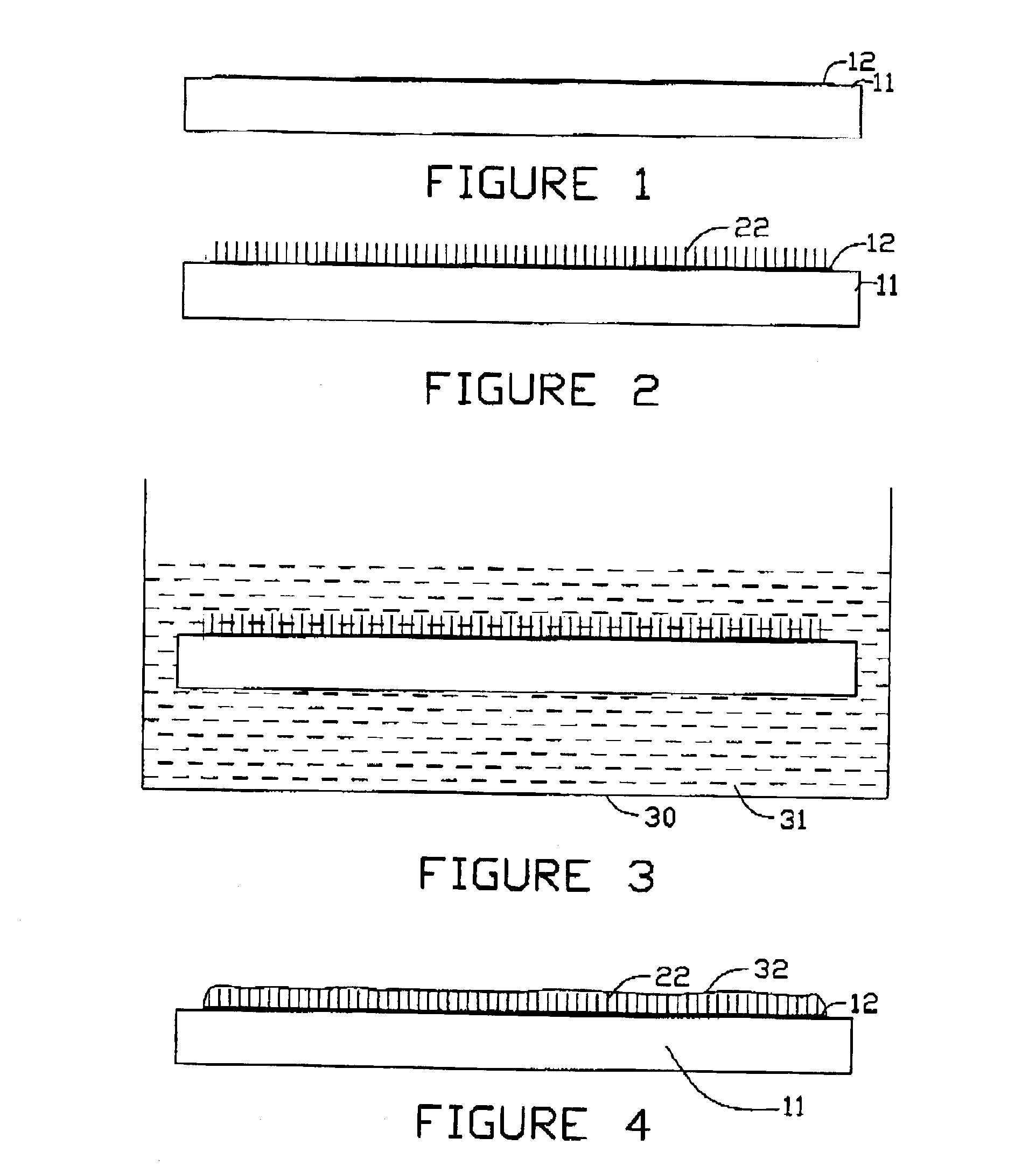
[0022]Reference will now be made to the drawings to describe the present invention in detail.

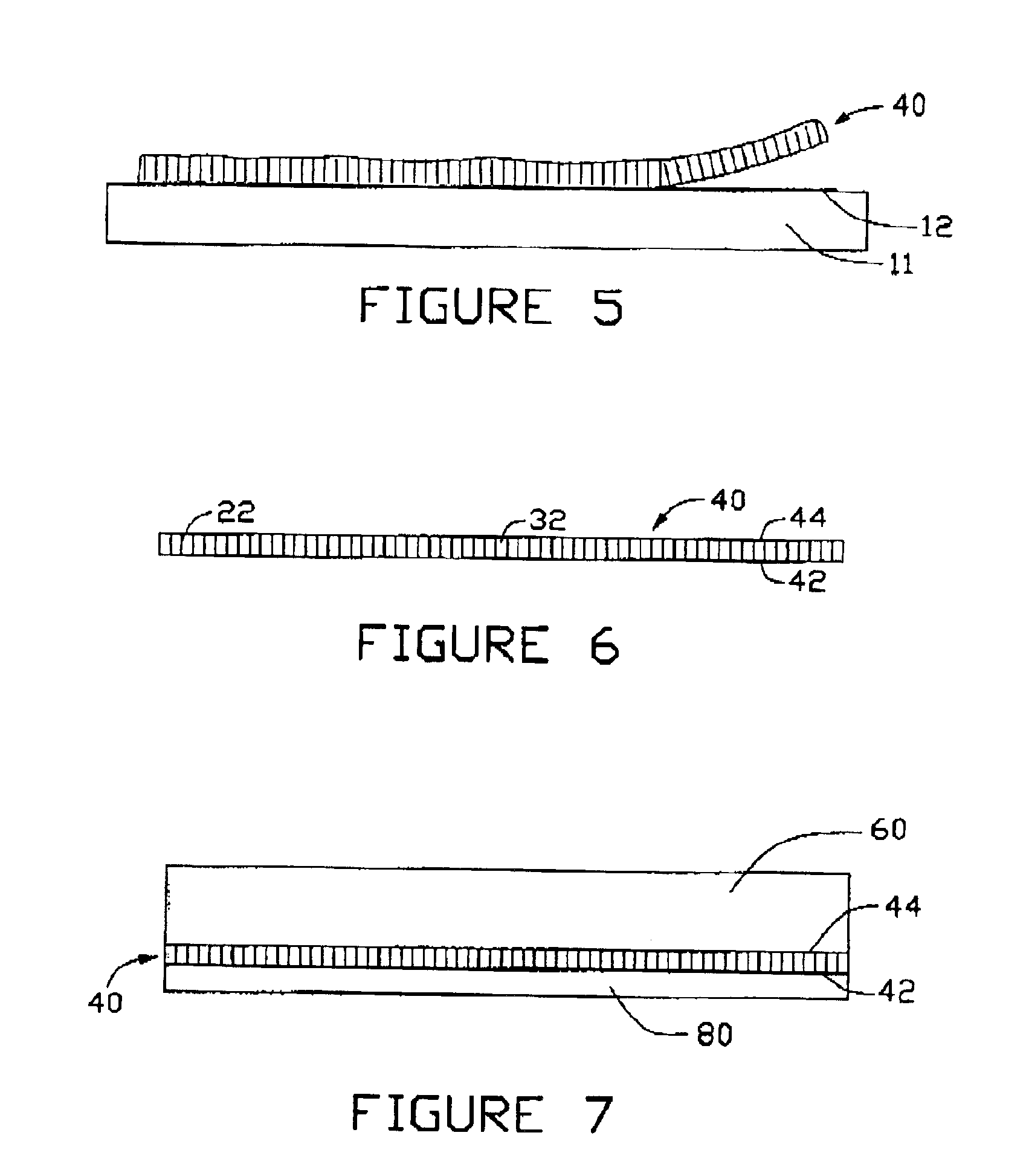
[0023]Referring to FIG. 6, a thermal interface material 40 in accordance with a preferred embodiment of the present invention comprises a polymer matrix 32 having a thermally conductive first face 42 and an opposite thermally conductive second face 44. An array of carbon nanotubes 22 is incorporated in the polymer matrix 32. The carbon nanotubes 22 are substantially parallel to each other, and extend between the first and second faces 42, 44.

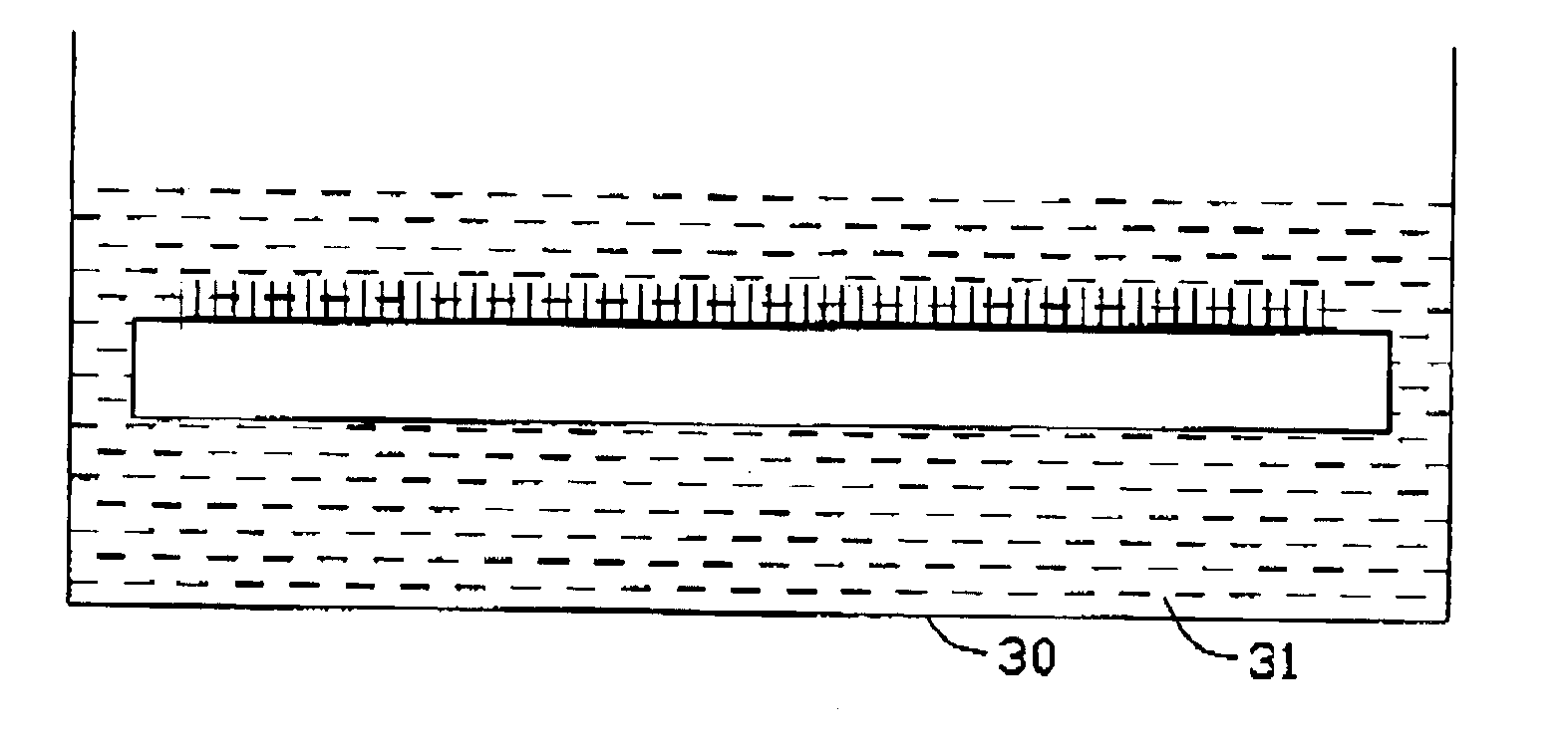
[0024]Referring also to FIGS; 1-5, a preferred method for making the thermal interface material 40 comprises the steps of:[0025](1) providing a substrate 11, and forming the array of carbon nanotubes 22 on the substrate 11;[0026](2) immersing the carbon nanotubes 22 in a liquid prepolymer 31 such that the liquid prepolymer 31 infuses into the array of carbon nanotubes 22;[0027](3) polymerizing the liquid prepolymer 31 to obtain the polymer matrix 32 havi...


PUM

PropertyMeasurementUnit
thicknessaaaaaaaaaa
thickaaaaaaaaaa
temperatureaaaaaaaaaa

Abstract

A thermal interface material (40) includes a polymer matrix (32) and an array of carbon nanotubes (22) incorporated in the polymer matrix. The polymer matrix has a thermally conductive first face (42) and an opposite thermally conductive second face (44). The carbon nanotubes are substantially parallel to each other, and extend between the first and the second faces. A preferred method for making the thermal interface material includes the steps of: (a) forming the array of carbon nanotubes on a substrate (11); (b) immersing the carbon nanotubes in a liquid prepolymer (31) such that the liquid prepolymer infuses into the array of carbon nanotubes; (c) polymerizing the liquid prepolymer to obtain the polymer matrix having the carbon nanotubes secured therein; and (d) peeling the polymer matrix having the carbon nanotubes off from the substrate to obtain the thermal interface material.

Description

BACKGROUND OF THE INVENTION[0001]1. Field of the Invention[0002]The present invention relates to a thermal interface material and a method for making the same, especially to a thermal interface material made from carbon nanotubes and a method for making such a material.[0003]2. Description of Related Art[0004]Nowadays semiconductor devices are smaller and run faster than ever before. These devices also generate more heat than ever before. A semiconductor device should be kept within its operational temperature limits to ensure good performance and reliability. Typically, a heat sink is attached to a surface of the semiconductor device. Heat is transferred from the semiconductor device to ambient air via the heat sink. When attaching the heat sink to the semiconductor device, respective surfaces thereof are brought together into intimate contact. No matter how precisely the heat sink and semiconductor device are manufactured, as much as 99% of the respective surfaces are separated by...

Claims


Application Information

Patent Timeline
Patent Type & Authority Patents(United States)
IPC IPC(8): C08K7/24C08K7/00C01B31/02C08K3/04C08L75/04C08L101/00H01L23/373
CPCB82Y30/00C08K7/24C08K2201/011Y10S977/753C08K3/041H01L23/373H01L2924/0002H01L2924/00C08L75/08
Inventor FAN, SHOUSHANLIU, PAO LOHUANG, HUALI, YOUNGDE
Owner TSINGHUA UNIV
Why Eureka
Try Eureka