Differential to single-ended logic converter

a logic converter and converter technology, applied in the direction of logic circuit coupling/interface arrangement, multi-input and output pulse circuits, pulse techniques, etc., can solve the problem of relatively high current consumption of current mode logic circuits, and achieve the effect of convenient implementation

Inactive Publication Date: 2005-08-02
LONGITUDE SEMICON S A R L
View PDF5 Cites 59 Cited by
  • Summary
  • Abstract
  • Description
  • Claims
  • Application Information

AI Technical Summary

Benefits of technology

[0016]In an alternative embodiment of the converter stage according to the invention the pairs of resistors are replaced by pairs of MOS transistors wherein the first pair of resistors is replaced by the source-drain paths of two NMOS transistors being connected in series between the gate terminal of the first PMOS transistor and the gate terminal of the second PMOS transistor. The gate terminals of the two pair-NMOS transistors are connected to a supply voltage. The second pair of resistors is replaced by the source-drain paths of a pair of PMOS transistors connected in series between the gate terminal of the first NMOS transistor and the gate terminal of the second NMOS transistor. The gate terminals of the two pair-PMOS transistors are connected to ground potential. An advantage of this alternative embodiment is that transistors are significantly easier to implement in CMOS circuits than conventional resistors.
[0017]In yet another preferred embodiment of the inventive converter stage inverter stages are connected to the outputs. This embodiment has the advantage that the single-ended output signals are more stable and cover a full swing between ground and supply voltage.

Problems solved by technology

However, current mode logic circuits have a relatively high current consumption because current flows through the transistors at all times. Therefore, CML logic circuits are employed where high speed is required, and they are combined with conventional CMOS circuits which operate slower but are less current consuming.

Method used


Image

  • Differential to single-ended logic converter
  • Differential to single-ended logic converter
  • Differential to single-ended logic converter

Examples


Embodiment Construction

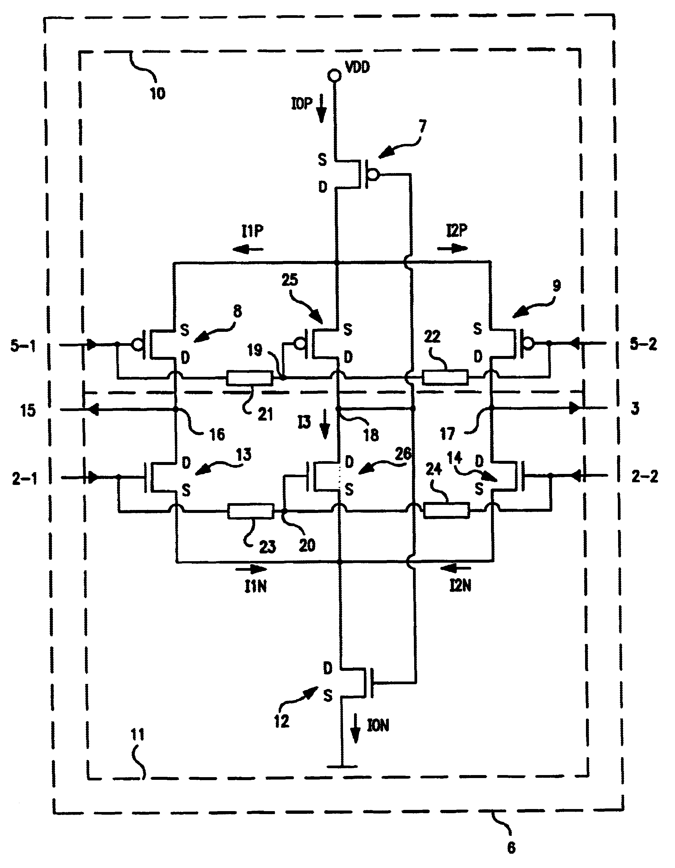
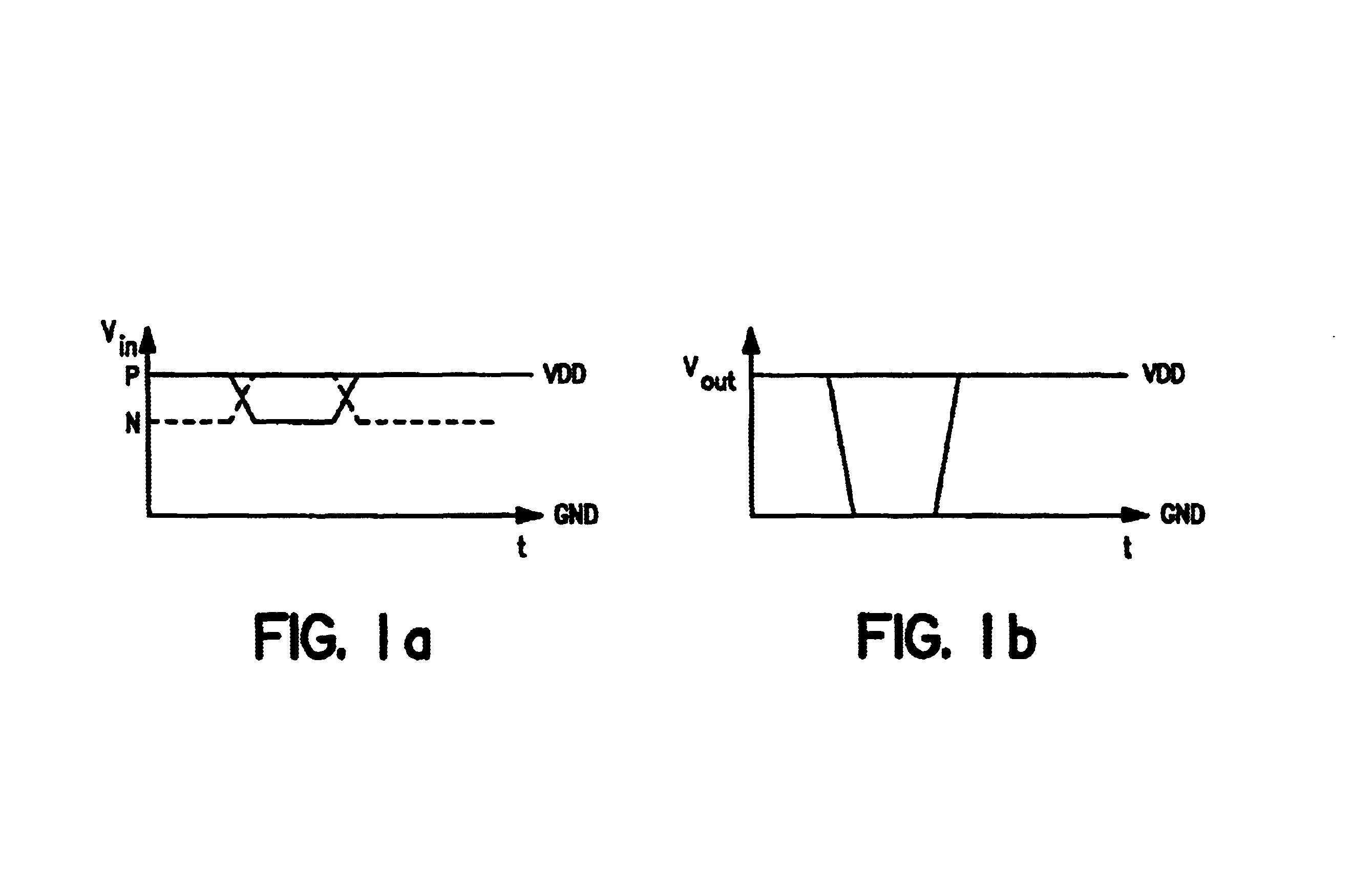
[0028]The present invention is a converter stage for converting a differential logic input signal and a corresponding common mode differential logic signal each having a first single-ended logic signal and a complementary second single-ended logic signal into a single-ended logic output signal.

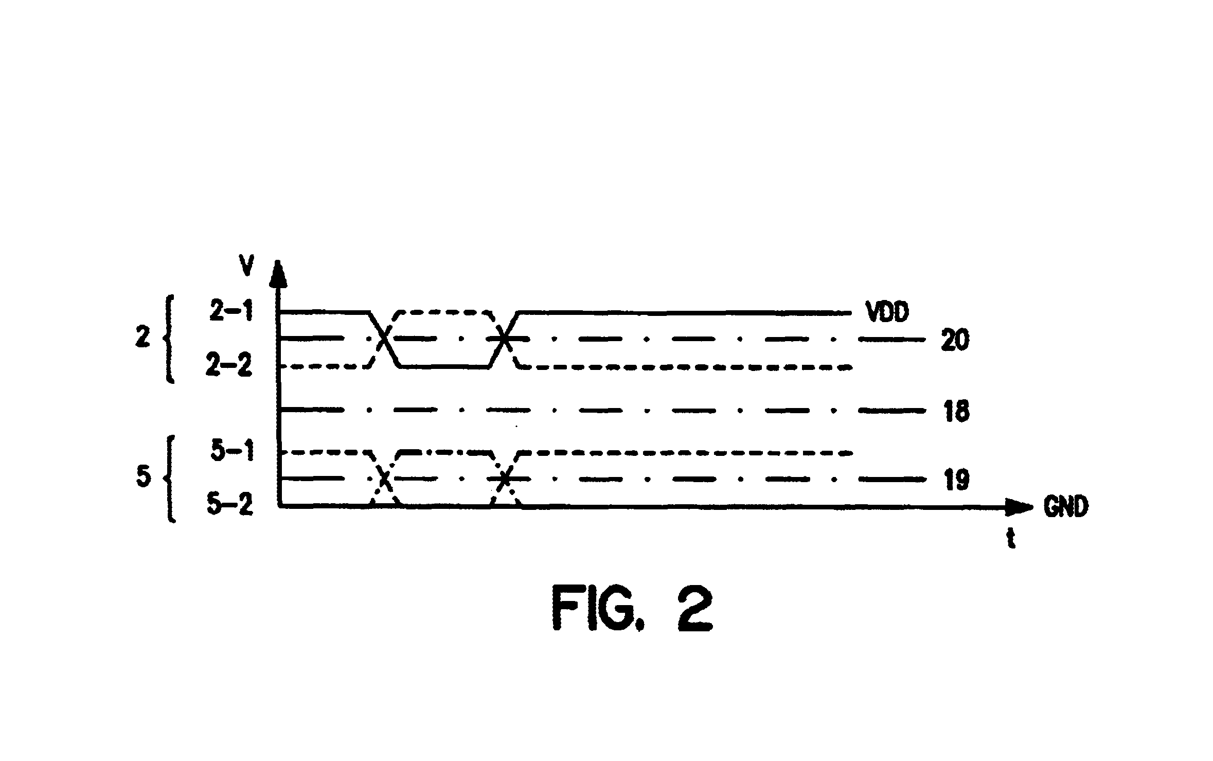
[0029]FIG. 2 shows a typical differential current mode logic signal 2 that comprises a first single-ended logic signal 2-1 and a complementary second single-ended logic signal 2-2, wherein the mid-potential 20 of the differential signal 2 is centered between the minimum and maximum voltage level of the signal 2 corresponding to the two logic levels. The corresponding common mode differential logic signal 5 comprises a first and a second single-ended logic signal 5-1, 5-2 each having a minimum voltage level and a maximum voltage level and a mid-potential centered in between 19. In the common mode logic signal 5 the minimum voltage level is usually referenced to ground GND. FIG. 2 further illust...


PUM


Abstract

The present invention is a converter stage for converting a differential logic input signal and a corresponding common mode differential logic signal each having a first single-ended logic signal and a complementary second single-ended logic signal into a single-ended logic output signal. The converter stage comprises a first and a second differential stage each having a first and a second MOS transistor and a first and second current source for the differential stages. According to the invention the current sources are controlled by the voltage level which is centered between the mid-potentials of the common mode level differential logic signal and the mid-potential of the differential logic input signal.

Description

TECHNICAL FIELD[0001]The present invention relates generally to voltage level converters. More particularly, the invention relates to a converter stage for converting a current mode differential logic level into a single-ended logic level.BACKGROUND OF THE INVENTION[0002]Current mode logic (CML) circuits are digital circuits where changes of logic levels are realized by switching currents instead of voltages. In MOS realizations of CML, the transistors used as switching elements are always in the saturation regime but the transistors remain within the active operating regions at all times. Thus, the transistors that are emitter coupled do not have a charge-storage time to content with and can change states very rapidly. An advantage of emitter coupled logic (ECL), or current mode logic (CML) respectively, is that it enables very high speed. However, current mode logic circuits have a relatively high current consumption because current flows through the transistors at all times. Ther...

Claims


Application Information

Patent Timeline
Patent Type & Authority Patents(United States)
IPC IPC(8): H03K19/0185H03K5/003H03K5/24
CPCH03K5/003H03K5/2481H03K19/018528
Inventor MULLER, DAVIDREBMANN, VOLKMAR
Owner LONGITUDE SEMICON S A R L
Why Eureka
Try Eureka