Apparatus and method extending flip-chip pad structures for wirebonding on low-k dielectric silicon

a dielectric silicon, flip-chip pad technology, applied in electrical apparatus, semiconductor devices, semiconductor/solid-state device details, etc., can solve the problems of cost, design, test, and qualification of additional features

Inactive Publication Date: 2005-08-09
TAHOE RES LTD
View PDF9 Cites 63 Cited by
  • Summary
  • Abstract
  • Description
  • Claims
  • Application Information

AI Technical Summary

Problems solved by technology

In designing rules for manufacturing chips having different geometries (such as smaller features of d...

Method used


Image

  • Apparatus and method extending flip-chip pad structures for wirebonding on low-k dielectric silicon
  • Apparatus and method extending flip-chip pad structures for wirebonding on low-k dielectric silicon
  • Apparatus and method extending flip-chip pad structures for wirebonding on low-k dielectric silicon

Examples


Embodiment Construction

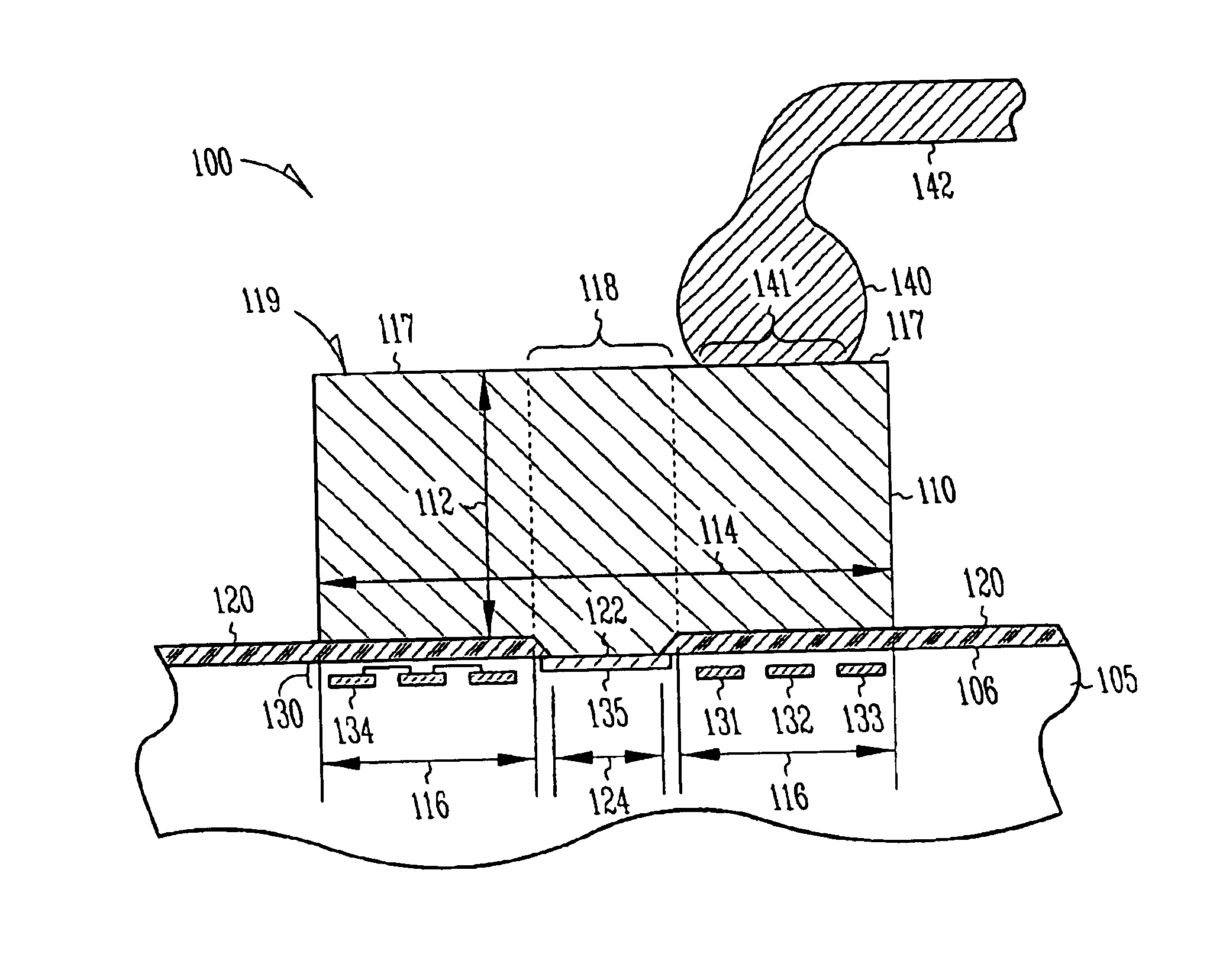
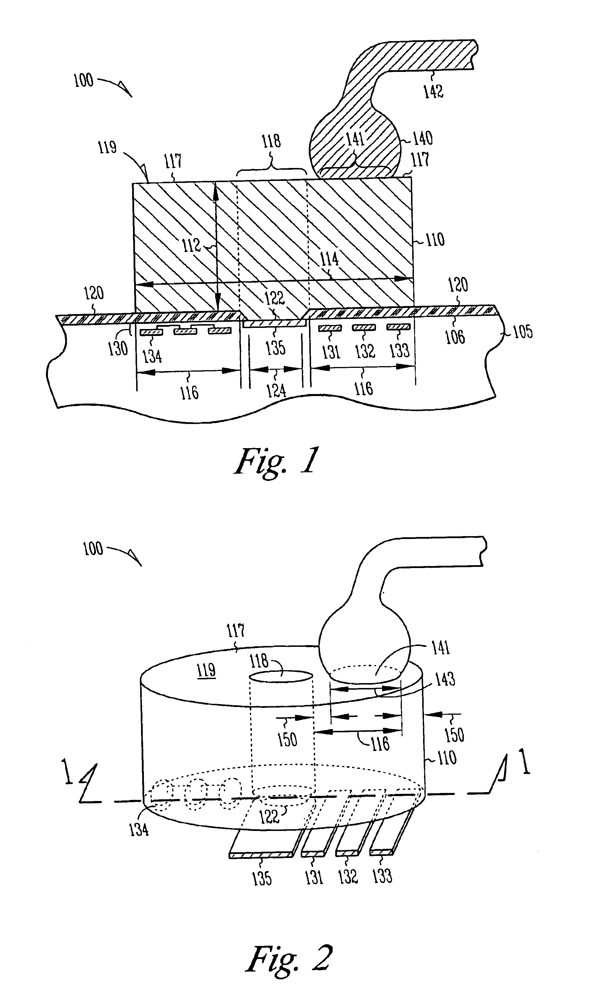
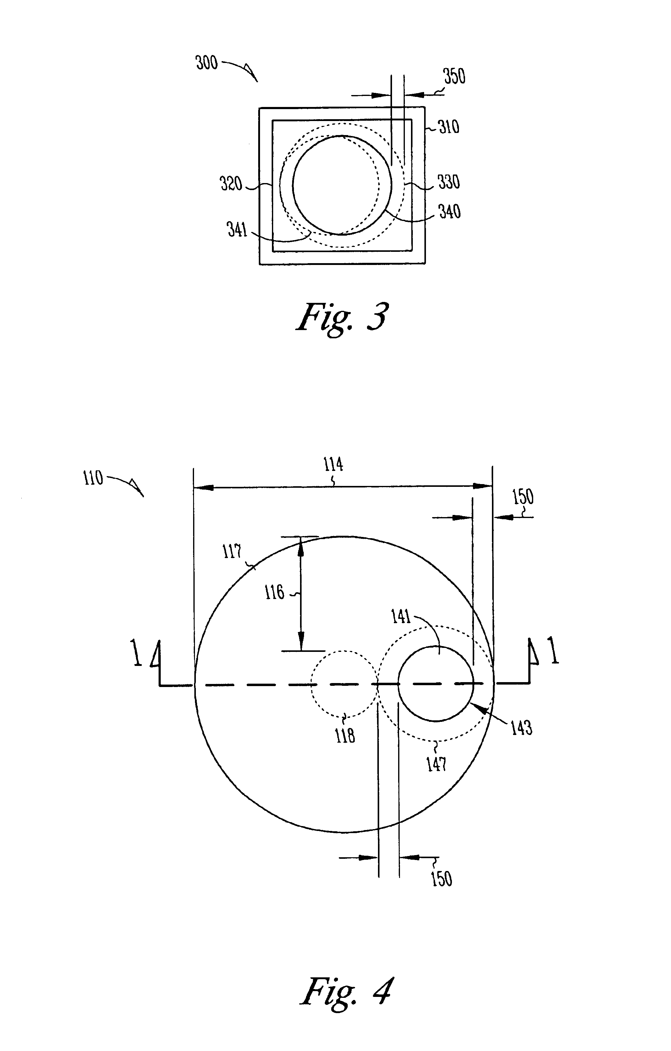
[0018]In the following detailed description of the preferred embodiments, reference is made to the accompanying drawings that form a part hereof, and in which are shown by way of illustration specific embodiments in which the invention may be practiced. It is understood that other embodiments may be utilized and structural changes may be made without departing from the scope of the present invention.

[0019]The leading digit(s) of reference numbers appearing in the Figures generally corresponds to the Figure number in which that component is first introduced, such that the same reference number is used throughout to refer to an identical component which appears in multiple Figures. The same reference number or label may refer to signals and connections, and the actual meaning will be clear from its use in the context of the description.

Terminology

[0020]The terms chip, die, integrated circuit, monolithic device, semiconductor device, and microelectronic device, are used interchangeably...


PUM


Abstract

A method and apparatus for making pad structures suitable for wirebonding and, optionally, also for solder-ball connections. Some embodiments include an electronics chip having a substrate with circuitry, a compliant electrically insulating layer deposited on at least a portion of the substrate, and an electrical connection pad, the pad having an electrical connection to the circuitry through an aperture in the insulating layer and a peripheral bonding zone region extending over the insulating layer. In some embodiments, the bonding zone is exclusively over the insulating layer outside of the aperture. In some embodiments, the pads are suitable for both solder-ball and wirebond connections. By making a wirebond connection to an area of a pad over the compliant insulating layer, the underlying circuitry is protected from ultrasonic energy of the bonding process.

Description

FIELD OF THE INVENTION[0001]This invention relates to the field of electronic package fabrication, and more specifically to a method and apparatus for making pad structures for wirebonding and / or solder-ball connections.BACKGROUND OF THE INVENTION[0002]Bare electronic chips typically need to be packaged in a package that provides an electric circuit between each electrical connection of the chip and an external connector such as a pin or a ball extending from the package to external circuitry such as a printed circuit board. In designing rules for manufacturing chips having different geometries (such as smaller features of devices such as wiling traces or transistors) it is costly to design, test, and qualify additional features. Chips that run at extremely high frequencies, e.g., upwards of 40 gigahertz, also have rule constraints as to the type, thickness, spacing, and layout of traces and signal pads required to provide adequate signal capability. Further, such chips typically ne...

Claims


Application Information

Patent Timeline
IPC IPC(8): H01L23/485H01L23/48
CPCH01L24/03H01L24/05H01L24/13H01L24/10H01L24/48H01L2224/0401H01L2224/48847H01L2224/48647H01L2924/01033H01L2924/01019H01L2924/20752H01L2924/20751H01L2924/14H01L2924/014H01L2924/01082H01L2924/01079H01L2924/01075H01L2924/0105H01L2924/01046H01L2924/01042H01L2924/01029H01L2924/01028H01L2924/01022H01L2924/01014H01L2924/01013H01L2924/01007H01L2224/85205H01L24/45H01L2224/04042H01L2224/04073H01L2224/05553H01L2224/05555H01L2224/05647H01L2224/13099H01L2224/45015H01L2224/45144H01L2224/45147H01L2224/45164H01L2224/48463H01L2224/85011H01L2924/00014H01L2924/00H01L2224/023H01L2224/13H01L2924/20755H01L2924/2075H01L2924/20754H01L2924/0001
Inventor MATHEW, RANJAN J.
Owner TAHOE RES LTD
Why Eureka
Try Eureka