Method and apparatus for processing a micro sample

a micro-sample and micro-processing technology, applied in the direction of material analysis using wave/particle radiation, semiconductor/solid-state device testing/measurement, instruments, etc., can solve the problems of reducing resolution, unable to cope with vertical observation, and inability to vertically observe the inner wall section of the hole or groove, etc., to achieve high throughput, high resolution, and high accuracy

Inactive Publication Date: 2005-08-09
HITACHI LTD
View PDF30 Cites 70 Cited by
  • Summary
  • Abstract
  • Description
  • Claims
  • Application Information

AI Technical Summary

Benefits of technology

[0008]Second, a reduction in resolution resulting from the slant observation becomes a serious problem. When slantingly emitting an electron beam to a wafer surface from above and to observe a section of an inner wall of a hole or groove, observation resolution in a direction perpendicular to the wafer surface, that is, of the section of the inner wall of the hole or groove is reduced. A reduction rate reaches approximately 15% at an angle of 30°, and 30% at an angle of around 45°, which is most frequently used. Miniaturization of recent semiconductor devices has reached the limit, and measurement of the dimension or shape with accuracy below a few nano meters is required. Required observation resolution is less than 3 nm, which falls a technical limit area of a scanning electron microscope. In addition, with high resolution of such degree, depth of focus is extremely shallow and focusing is achieved only in a range below some ten percent of 1 μm, so that an appropriate observation range of a vertical section of the device at the time of slant observation is often less than half of a required area. This problem can be solved by vertical observation. The vertical observation enables superior observation in focus on the whole observation area.
[0009]Third, the observation section exists on a wall surface of a minute hole or groove formed in the wafer, so that numeral density of secondary electrons coming out of the hole are reduced in comparison with those on the surface of the wafer. Thus, secondary electron detecting efficiency is reduced and it causes a reduction in S / N of a secondary electron image, inevitably resulting in a reduction in accuracy of the section observation.
[0013]In view of the above problems, the present invention has its object to provide a method and apparatus for processing and observing a minute sample, which can vertically observe an inner section of the sample to be observed, and can carry out observation and analysis with high resolution, high accuracy and high throughput without degradation resulting from exposure to the air and without failure.
[0014]Another object of the present invention is to provide a minute sample processing apparatus which requires minimum capacity of a vacuum container and a reduced occupying area and has high operability even when the apparatus is intended for a large sample. Still another object of the present invention will be described in embodiments described hereinafter.

Problems solved by technology

First, to observe a section of a hole or groove of the sample formed by FIB processing, a sample stage is inclined to thereby observe a section of an inner wall of the hole or groove in a slanting direction. In that case, an adjustment range of inclination of the sample stage is limited by constraints in structure due to a working distance of an FIB apparatus, presence of an objective lens, or size of a sample stage, and larger inclination cannot be allowed. Thus, vertical observation of the section of the inner wall of the hole or groove is impossible. The vertical observation of the section is indispensable in confirmation of processing properties such as dry etching, planarization, thin film forming, or the like in process development or the like of semiconductor device manufacturing, but the above described known apparatuses cannot cope with the vertical observation.
Second, a reduction in resolution resulting from the slant observation becomes a serious problem. When slantingly emitting an electron beam to a wafer surface from above and to observe a section of an inner wall of a hole or groove, observation resolution in a direction perpendicular to the wafer surface, that is, of the section of the inner wall of the hole or groove is reduced. A reduction rate reaches approximately 15% at an angle of 30°, and 30% at an angle of around 45°, which is most frequently used. Miniaturization of recent semiconductor devices has reached the limit, and measurement of the dimension or shape with accuracy below a few nano meters is required. Required observation resolution is less than 3 nm, which falls a technical limit area of a scanning electron microscope. In addition, with high resolution of such degree, depth of focus is extremely shallow and focusing is achieved only in a range below some ten percent of 1 μm, so that an appropriate observation range of a vertical section of the device at the time of slant observation is often less than half of a required area. This problem can be solved by vertical observation. The vertical observation enables superior observation in focus on the whole observation area.
Third, the observation section exists on a wall surface of a minute hole or groove formed in the wafer, so that numeral density of secondary electrons coming out of the hole are reduced in comparison with those on the surface of the wafer. Thus, secondary electron detecting efficiency is reduced and it causes a reduction in S / N of a secondary electron image, inevitably resulting in a reduction in accuracy of the section observation.

Method used


Image

  • Method and apparatus for processing a micro sample
  • Method and apparatus for processing a micro sample
  • Method and apparatus for processing a micro sample

Examples


embodiment 1

(Embodiment 1)

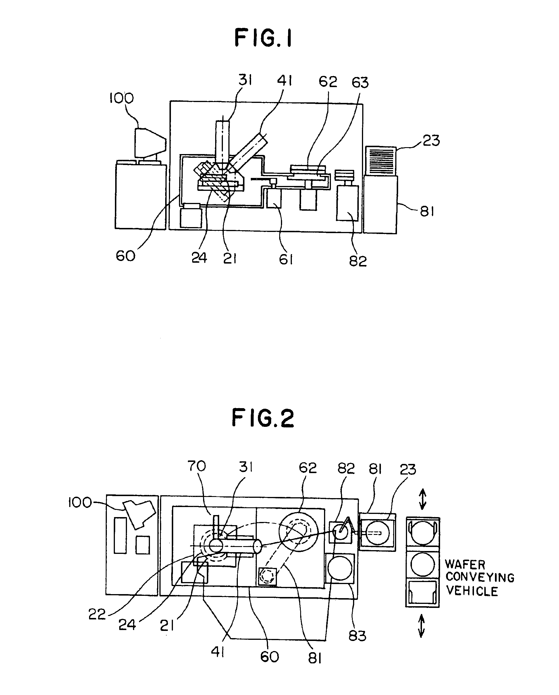
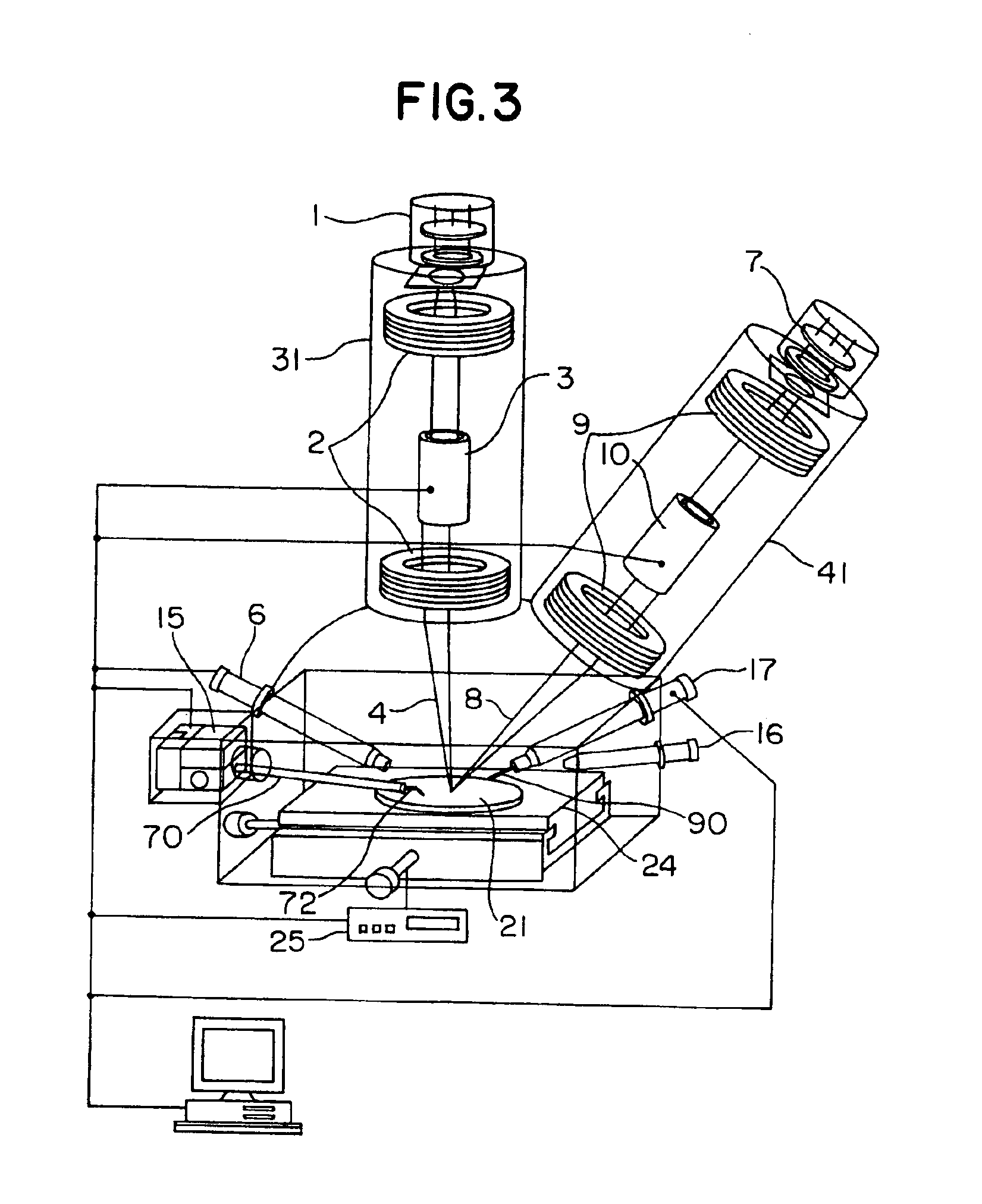
[0048]A structure and an operation of a first embodiment of an apparatus of the invention will be described with reference to FIGS. 1, 2 and 3. FIGS. 1 and 2 show a whole structure of the apparatus and FIG. 3 shows structures of a focused ion beam optical system, scanning electron microscope optical system and around a sample stage in detail. Shown in this embodiment is a wafer corresponding apparatus in the minute sample processing and observation apparatus of the present invention. FIG. 3 shows a schematic bird's eye section of FIG. 1, and there are some differences between the figures, though not essential, in orientations or details of apparatuses for convenience in description. In FIG. 1, around a center of an apparatus system are appropriately located a focused ion beam optical system 31 and an electron beam optical system 41 above a vacuum sample chamber 60. A sample stage 24 on which a wafer 21 to be a sample is placed is located inside the vacuum sample chambe...

embodiment 2

(Embodiment 2)

[0077]A structure and an operation of a minute sample processing and observation apparatus according to a second embodiment of the present invention will be described with reference to FIGS. 6 and 7. FIG. 7 is a plan view of FIG. 6, and there are some differences between the figures in orientations or details of apparatuses for convenience in description but they are not essential differences. In this apparatus, a focused ion beam optical system 31 is vertically disposed and a second focused ion beam optical system 32 is located at an angle of approximately 40° at the upper part of a vacuum sample chamber 60 disposed in the central part of the apparatus system. An electron beam optical system 41 is slantingly located at an angle of approximately 45°. Three optical systems 31, 32, 41 are adjusted in such a manner that their respective central axes intersect at a point around a surface of a wafer 21. Similarly to the apparatus of the first embodiment, inside the vacuum s...

embodiment 3

(Embodiment 3)

[0081]A structure and an operation of a minute sample processing and observation apparatus according to a third embodiment of the present invention will be described with reference to FIGS. 8 and 9. FIG. 9 is a plan view of FIG. 8, and there are some differences between the figures in orientations or details of apparatuses for convenience in description but they are not essential difference. In the apparatus of this embodiment, a focused ion beam optical system 33 is slantingly located at an angle of approximately 45° at an upper portion of a vacuum sample chamber 60 disposed at the central part of the apparatus system. An electron beam optical system 42 is also slantingly located at an angle of approximately 45°. Two optical systems 33, 42 are adjusted in such a manner that their respective central axes intersect at a point around a surface of a wafer 21. Similarly to the apparatus of the first embodiment, inside the vacuum sample chamber 60 is located a sample stage ...


PUM

PropertyMeasurementUnit
diameteraaaaaaaaaa
diameteraaaaaaaaaa
depthaaaaaaaaaa

Abstract

An object of the invention is to realize a method and an apparatus for processing and observing a minute sample which can observe a section of a wafer in horizontal to vertical directions with high resolution, high accuracy and high throughput without splitting any wafer which is a sample. In an apparatus of the invention, there are included a focused ion beam optical system and an electron optical system in one vacuum container, and a minute sample containing a desired area of the sample is separated by forming processing with a charged particle beam, and there are included a manipulator for extracting the separated minute sample, and a manipulator controller for driving the manipulator independently of a wafer sample stage.

Description

[0001]This is a continuation of application Ser. No. 09 / 960,479 filed 24 Sep. 2001, now U.S. Pat. No. 6,781,125 which claims priority to Japanese Patent Application No. 2000-340387 filed 2 Nov. 2000, the contents of which are incorporated herein by reference in their entirety.BACKGROUND OF THE INVENTION[0002]The present invention relates to an apparatus system used as observation, analysis and evaluation means in research and development and manufacturing of an electronic device such as a semiconductor device, liquid crystal device and a magnetic head, a micro-electronic device or the like which require observation and analysis of not only a surface of an object to be observed but also an inner section near the surface.[0003]In manufacturing of a semiconductor device such as a semiconductor memory typified by a dynamic random access memory, a microprocessor and a semiconductor laser, and electronic parts such as a magnetic head, a product property is inspected for quality control of...

Claims


Application Information

Patent Timeline
Patent Type & Authority Patents(United States)
IPC IPC(8): H01J37/305H01J37/256H01J37/252H04L29/06H04L29/08G01N1/28G01N23/225G01N1/32G01Q10/00G01Q30/02G01Q30/04G01Q30/16G01Q30/20H01J37/20H01J37/28H01J37/30H01J37/317H01L21/66
CPCG01N23/225H01J37/256H01J37/3056H04L29/06H04L67/16H01J2237/20H01J2237/202H01J2237/31745H04L69/329H04L67/51H04L9/40
Inventor TOKUDA, MITSUOFUKUDA, MUNEYUKIMITSUI, YASUHIROKOIKE, HIDEMITOMIMATSU, SATOSHISHICHI, HIROYASUKASHIMA, HIDEOUMEMURA, KAORU
Owner HITACHI LTD
Why Eureka
Try Eureka