Ballasting MOSFETs using staggered and segmented diffusion regions

a diffusion region and mosfet technology, applied in the field of mosfets, can solve the problems of metal opening, esd is a significant problem, integrated circuits (ics), etc., and achieve the effect of increasing the resistance seen by the hot spot filament, adding series resistance, and increasing the total resistance of the mos

Inactive Publication Date: 2005-08-09
SYNAPTICS INC
View PDF7 Cites 37 Cited by
  • Summary
  • Abstract
  • Description
  • Claims
  • Application Information

AI Technical Summary

Benefits of technology

[0010]The present invention provides MOSFET-based ESD protection devices that add series resistance to the path that a hot spot filament current must take by requiring the current to flow both laterally and vertically in going from the drain contacts to the source contacts. This construction also adds to the total resistance of the MOSFET thereby extending the failure voltage of a MOSFET in snap-back which allows multiple fingers to trigger. This is achieved by segmenting the active or diffusion areas in both the drain and the source, and staggering the segments so that drain segments are not opposite source segments. Since the drain and source diffusion segments are offset (staggered), the filament current path is lengthened and includes lateral and vertical components, and the resistance seen by the hot spot filament is accordingly increased.

Problems solved by technology

In the world of electronic devices and in particular integrated circuits (ICs), ESD is a very significant problem.
The heat generated by ESD can cause metal to open due to melting, junction electrothermal shorts, oxide rupture or other serious damage to the IC components.
Susceptibility to ESD increases with the shrinking size of technology, and components directly connected to the I / O pads are particularly vulnerable.
Without a ballast resistance, one section may trigger ahead of others and become destroyed before other sections turn on.
Second, current and heat build-up in channel regions reaching the critical temperature is limited.
One problem with prior art ESD protection devices such as NFET 20 is that the ballasting region is long and space consuming.
NFET 20 is susceptible to failure as a result of the formation of hot spots during snapback.
The exponential relationship between carrier density and temperature and the resulting decrease in regional resistance with increasing temperature results in thermal “runaway”.

Method used


Image

  • Ballasting MOSFETs using staggered and segmented diffusion regions
  • Ballasting MOSFETs using staggered and segmented diffusion regions
  • Ballasting MOSFETs using staggered and segmented diffusion regions

Examples


Embodiment Construction

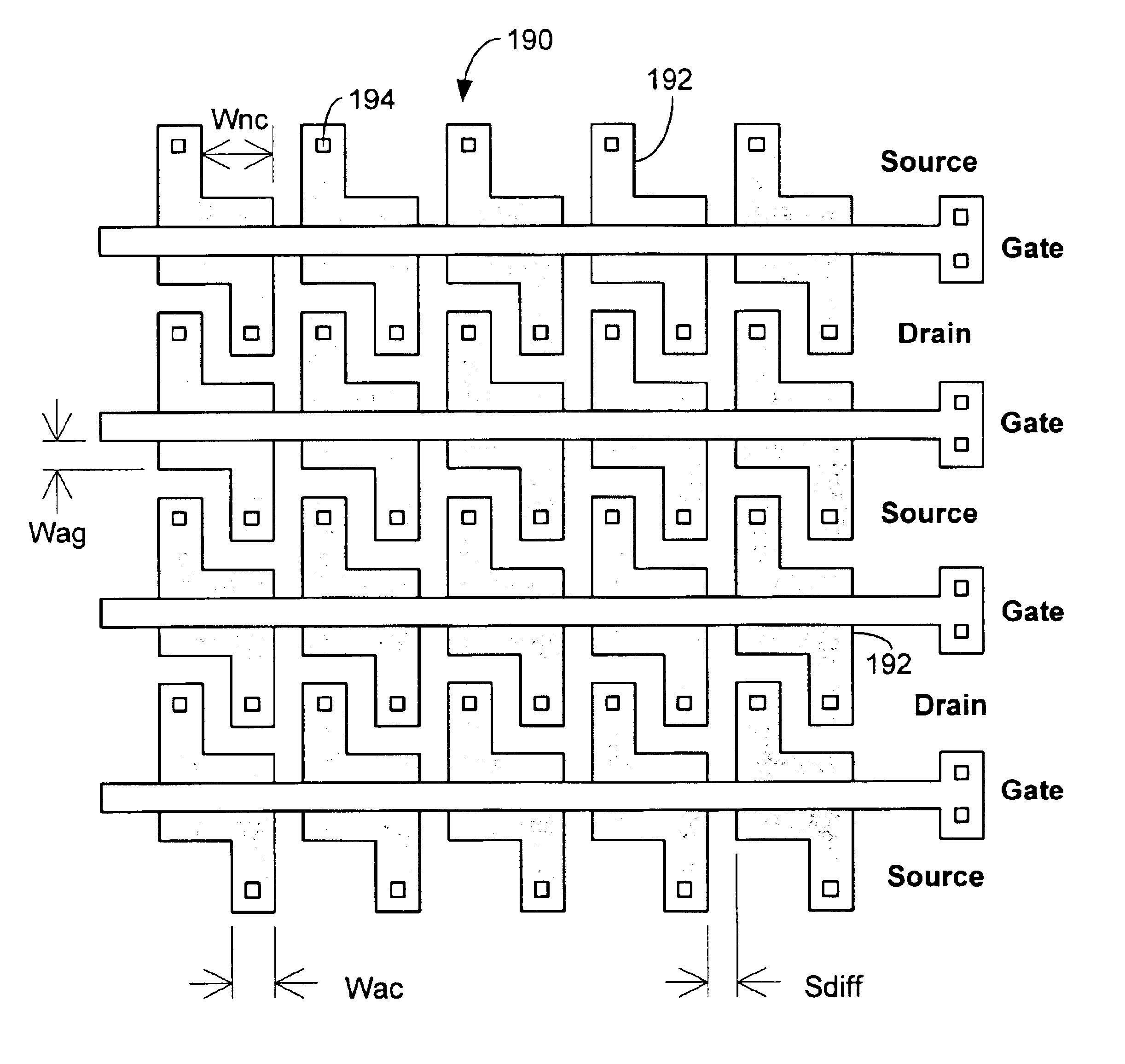
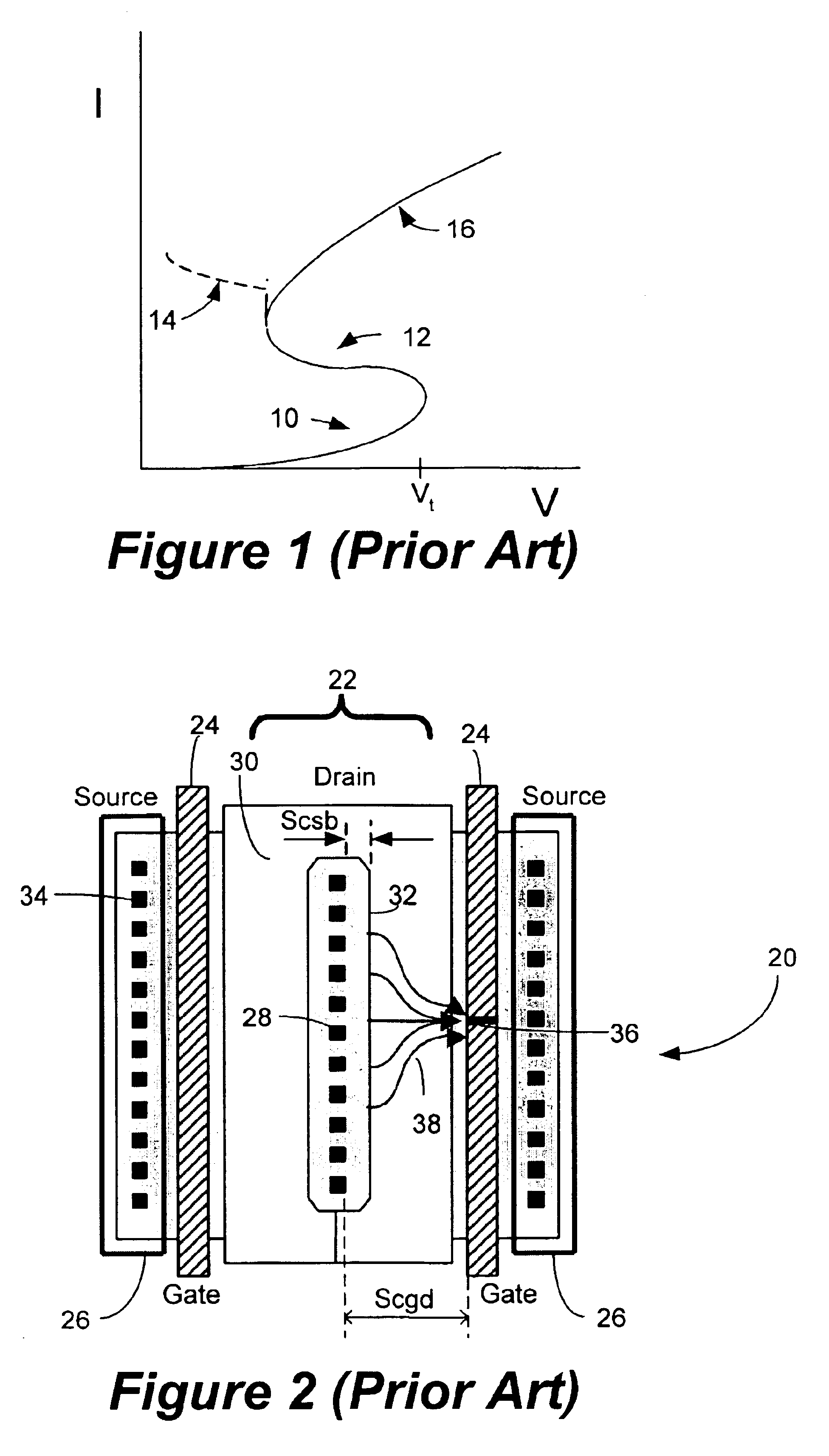
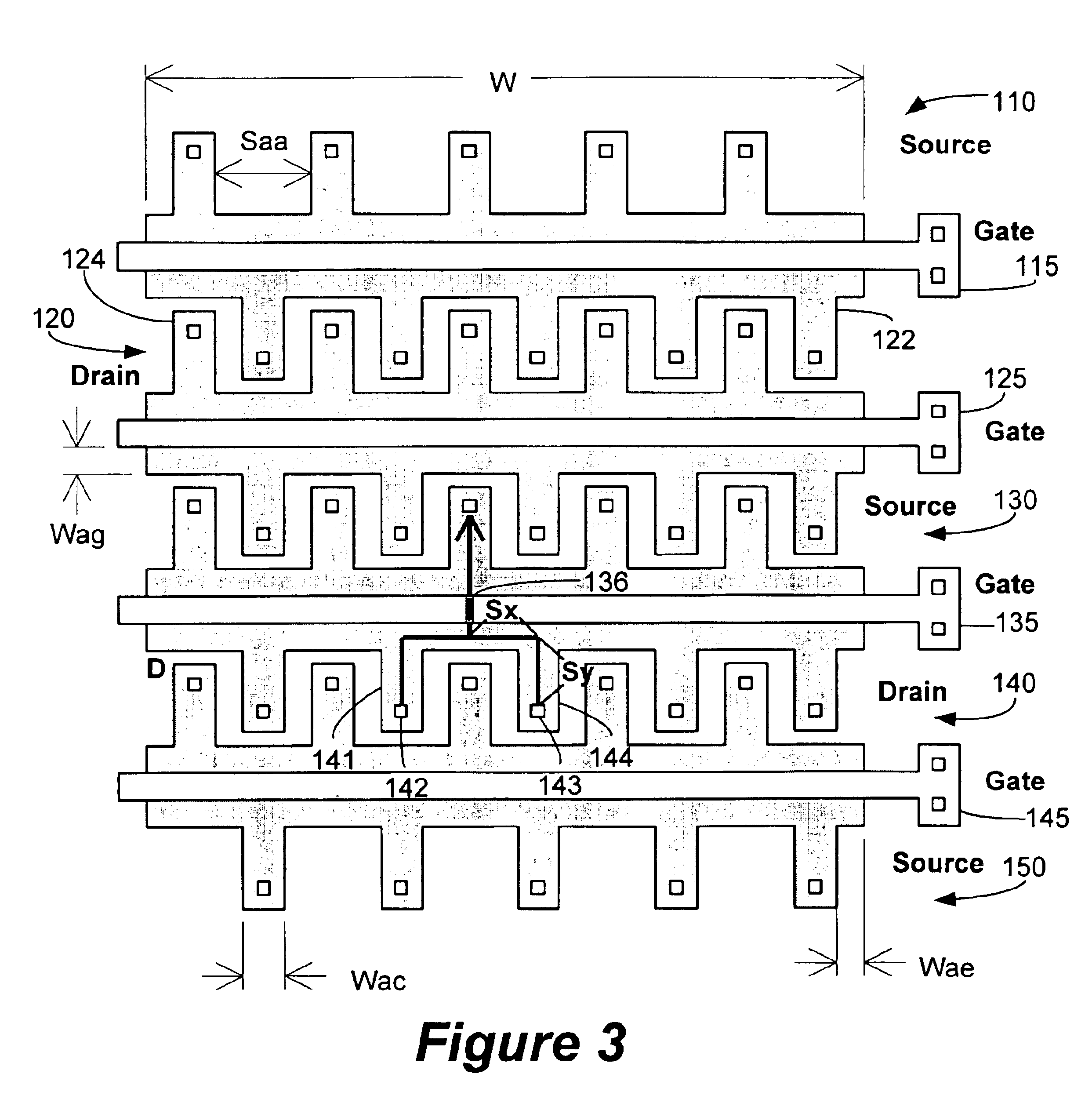
[0026]The present invention provides an improved MOSFET-type ESD protection device in which resistance is added to the path that a hot spot filament current must take by requiring the current to flow both laterally and vertically in going from the drain contacts to the source contacts. This is achieved by segmenting the active or diffusion areas in both the drain and the source, and staggering the segments so that drain segments and contacts are not opposite source segments and contacts. Since the drain and source diffusion segments are offset (staggered), the filament current path is lengthened and includes lateral and vertical components, and the resistance seen by filament hot spots is accordingly increased.

[0027]One embodiment of the present invention is illustrated in FIG. 3. Multi-finger MOSFET device 100 includes gates 115, 125, 135 and 145, sources 110, 130 and 150, and drains 120 and 140. Hence, a first FET is defined by source 110, gate 115 and drain 120; a second FET is d...


PUM


Abstract

An ESD protection circuit includes a field effect transistor device configured such that current flowing through a hot spot filament formed in a gate region must flow in a non-linear path from a drain contact to a source contact. Source diffusion areas are segmented and staggered relative to drain diffusion areas in order to provide the non-linear current path.

Description

FIELD OF THE INVENTION[0001]The present invention relates to MOSFETs used in ESD protection circuitry and, more particularly, relates to MOSFETs having staggered and segmented diffusion regions to lengthen the filament current path.BACKGROUND OF THE INVENTION[0002]Electrostatic discharge (ESD) is the spontaneous and rapid transfer of electrostatic charge between two objects having different electrostatic potentials. Familiar examples of ESD range from the relatively harmless, such as the shock one might receive after shuffling across a carpet and touching a doorknob, to the extreme, such as a lightning bolt. In the world of electronic devices and in particular integrated circuits (ICs), ESD is a very significant problem. The heat generated by ESD can cause metal to open due to melting, junction electrothermal shorts, oxide rupture or other serious damage to the IC components. Susceptibility to ESD increases with the shrinking size of technology, and components directly connected to ...

Claims


Application Information

Patent Timeline
Patent Type & Authority Patents(United States)
IPC IPC(8): H01L29/76H01L29/78H01L29/66H01L27/02H01L29/06H01L29/08
CPCH01L29/0692H01L29/0696H01L29/0847H01L29/78H01L29/7835
Inventor WORLEY, EUGENE R.
Owner SYNAPTICS INC
Why Eureka
Try Eureka