
Stack arrangement of a memory module

a memory module and stack arrangement technology, applied in the field of stack arrangement of memory modules, can solve the problems of relative high loss rate, and achieve the effects of reducing the number of transistors, and shortening the signal transit tim

Active Publication Date: 2005-08-09
POLARIS INNOVATIONS LTD
View PDF12 Cites 30 Cited by
  • Summary
  • Abstract
  • Description
  • Claims
  • Application Information

AI Technical Summary

Benefits of technology

"The present invention provides a solution for stacking memory modules by using a metallic coating on the bond pads of the memory chips and a protective structure called encapsulation. The metallic coating makes it possible to stack the memory chips with their central single-row, double-row, or multi-row bond pads by connecting them via suitable line conductor structures to the edge areas of the memory chips. The encapsulation acts as a spacer between the memory chips and the carrier substrate, and the orientation of the memory chips is the same as the orientation of the carrier substrate. This avoids interactions between wire bond connections. The invention also allows for the use of standard equipment and programs for manufacturing and testing the discrete components, as well as the use of sacrificial balls for testing. The invention further provides a stack arrangement in which the discrete components are stacked face down on the carrier substrate, with an additional reroute layer for direct electrical connection to the carrier substrate."

Problems solved by technology

In addition to prolonging the signal transit times, this design leads to technical problems because of the potential mechanical, electrical or thermal interactions between the wire bond connections at the crossover points.
Another serious disadvantage of this stack arrangement is that bum-in and testing are possible only once the stack arrangement has been completely assembled, which leads to a relatively high loss rate which amounts to approximately the square of the loss rate of one discrete component.

Method used


Image

  • Stack arrangement of a memory module
  • Stack arrangement of a memory module
  • Stack arrangement of a memory module

Examples


Embodiment Construction

[0024]The making and using of the presently preferred embodiments are discussed in detail below. It should be appreciated, however, that the present invention provides many applicable inventive concepts that can be embodied in a wide variety of specific contexts. The specific embodiments discussed are merely illustrative of specific ways to make and use the invention, and do not limit the scope of the invention.

[0025]The present invention will be described with respect to preferred embodiments in a specific context, namely a stacked memory module. The invention may also be applied, however, to other electronic components including other semiconductor devices such as processors and logic devices.

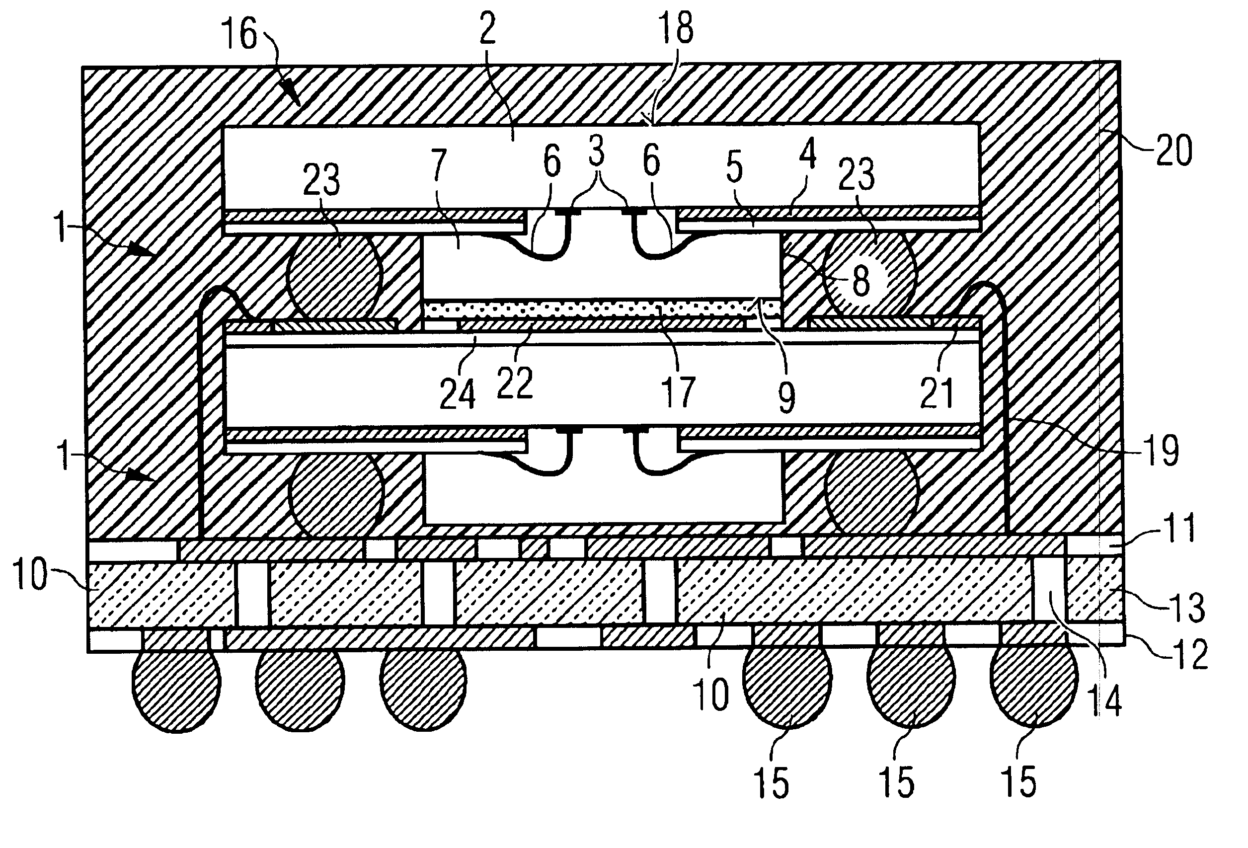
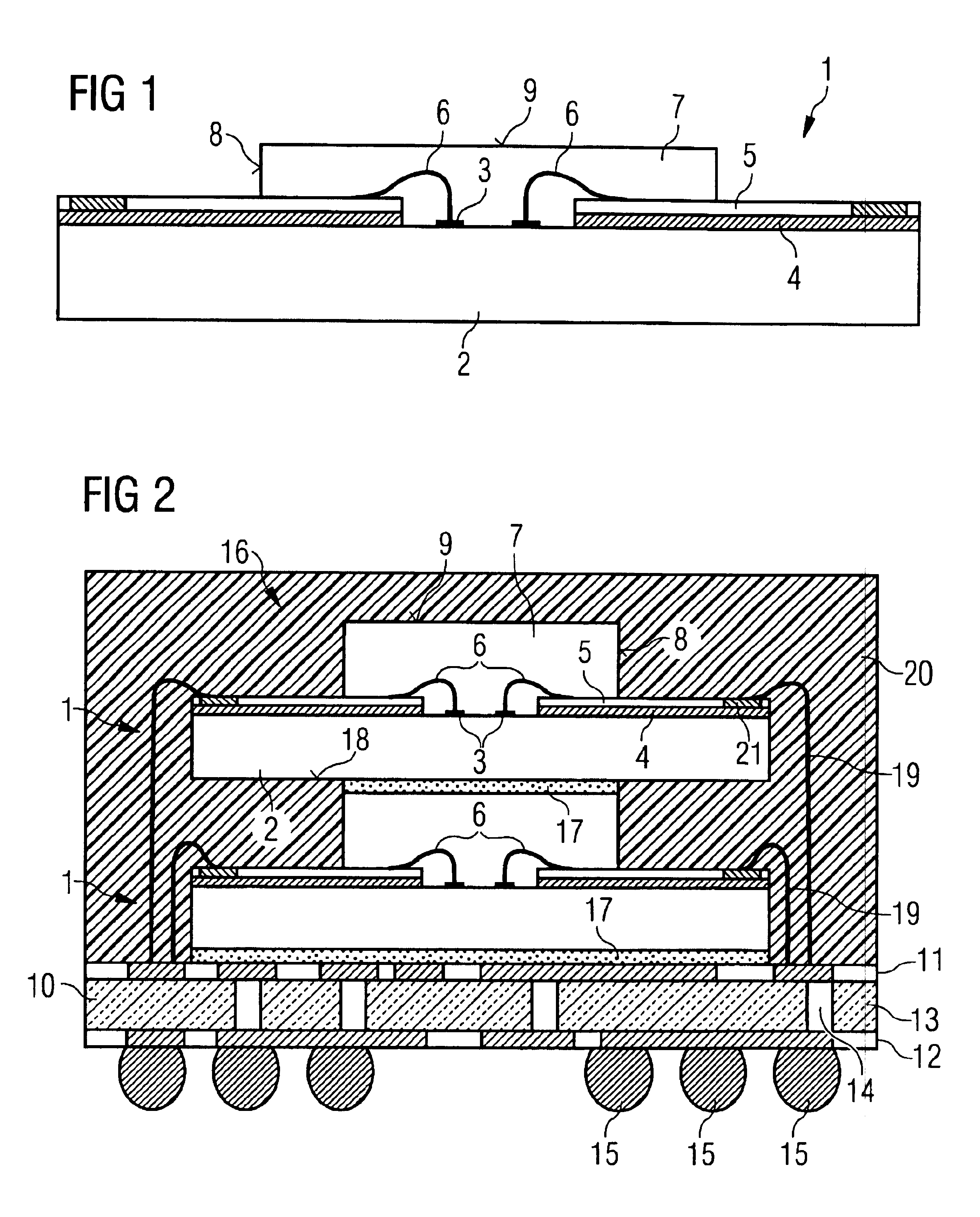
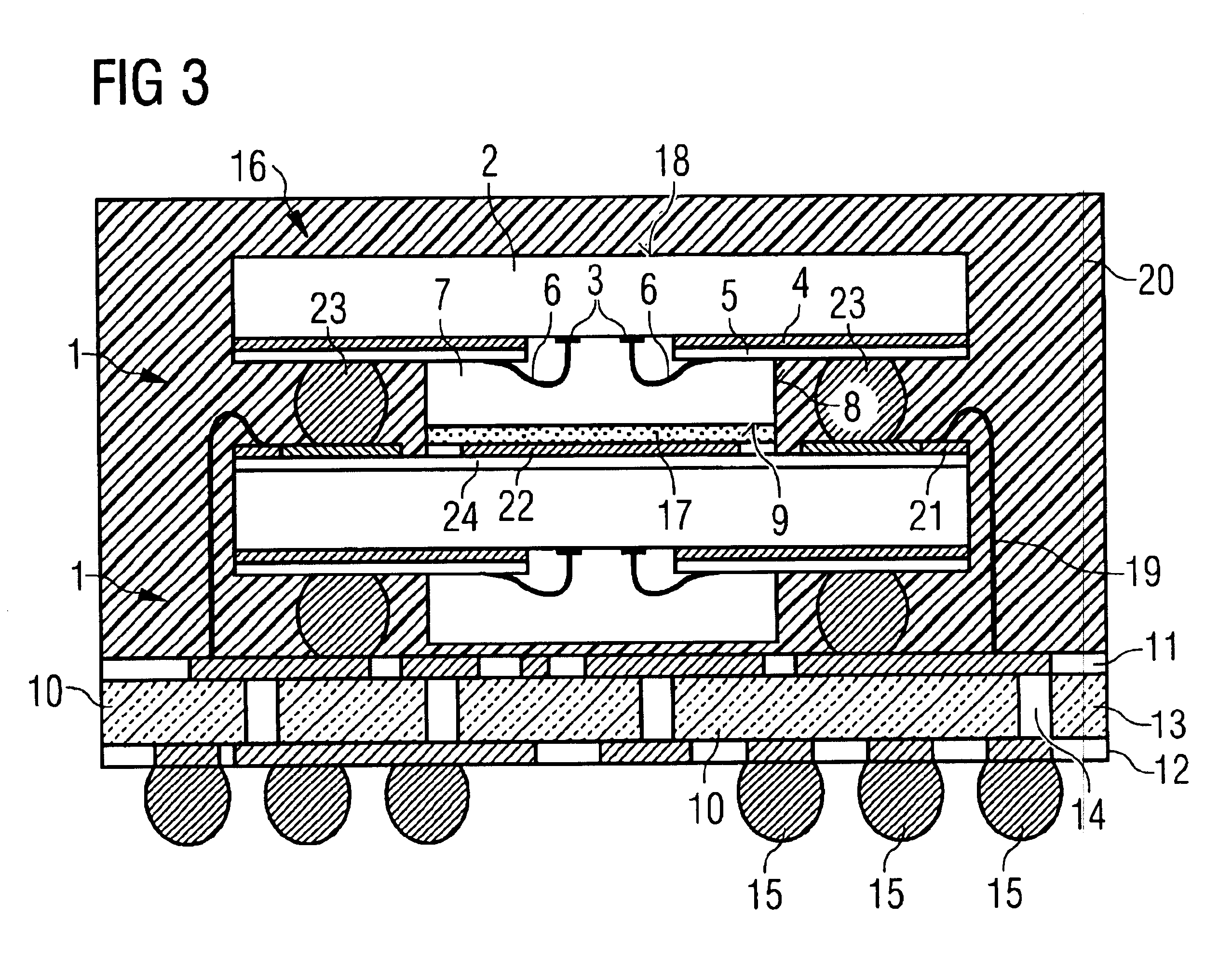
[0026]FIG. 1 shows discrete component 1, which is used to construct a stack arrangement according to embodiments of the present invention, two of which are shown in FIGS. 2 and 3. Discrete component 1 comprises a semiconductor (e.g., memory) chip 2 with double-row central bond pads 3, a metal...


PUM


Abstract

A stack arrangement of discrete components includes a carrier substrate and at least two discrete components, e.g., memory chips. The carrier substrate has line conductor structures and contact pads. Each of the discrete components includes centrally disposed bond pads and a metallic coating, which is electrically connected to the centrally disposed bond pads. The metallic coating is disposed on an active surface area of each discrete component. A protective structure overlies a central region of the discrete component. In the preferred embodiment, the metallic coatings of each discrete component are identical. Preferably, the discrete components are stacked on the carrier substrate so as to have the same orientation, so that the protective structure serves as a spacer between the discrete components. Further, the metallic coating is electrically coupled to the carrier substrate.

Description

CROSS-REFERENCE TO RELATED APPLICATIONS[0001]This application relates to the following co-pending and commonly assigned patent application Ser. No. 10 / 701,742, filed Nov. 4, 2003 and entitled “Method for Producing a Stack Arrangement of a Memory Module,” which application is hereby incorporated herein by reference.TECHNICAL FIELD[0002]The present invention relates generally to assembly of electronic components, and more particularly to a stack arrangement of a memory module.BACKGROUND[0003]A well-known embodiment of a stack arrangement provides for stacking two memory chips within an FBGA package. Here, the lower memory chip, with its active surface area face-down, is integrated into the circuit by means of the conventional Board-on-Chip (BoC) technology and the upper memory chip, with its active surface area face-up, is attached to the lower memory chip and integrated by means of wire bond connections.[0004]Since the electrical connections of the upper memory chip on the carrier su...

Claims


Application Information

Patent Timeline
Patent Type & Authority Patents(United States)
IPC IPC(8): H01L25/065
CPCH01L25/0657H01L2224/4824H01L2225/0651H01L2225/0652H01L2225/06527H01L2225/06575H01L2225/06582H01L2924/15311H01L2924/19107H01L2224/73215H01L2924/181H01L2224/8592H01L2924/00012
Inventor THOMAS, JOCHENHETZEL, WOLFGANG
Owner POLARIS INNOVATIONS LTD
Learn More