SEM profile and surface reconstruction using multiple data sets

a surface reconstruction and data set technology, applied in the direction of material analysis using wave/particle radiation, instruments, nuclear engineering, etc., can solve the problems of high processing defect rate, low precision and accuracy of estimation techniques, and high complexity of semiconductor manufacturing techniques for integrating circuits within semiconductor materials. achieve the effect of accurate estimation

Inactive Publication Date: 2005-08-16
KLA TENCOR TECH CORP
View PDF18 Cites 39 Cited by
  • Summary
  • Abstract
  • Description
  • Claims
  • Application Information

AI Technical Summary

Benefits of technology

[0007]The present invention is directed to an inspection technique capable of ac

Problems solved by technology

The industry of semiconductor manufacturing involves highly complex techniques for integrating circuits within semiconductor materials.
Due to the large scale of circuit integration and the decreasing size of semiconductor devices, the semiconductor manufacturing process is prone to processing defects.
Unfortunately, such a simple technique typically produces estimations having poor precision and accuracy.
However, many processes

Method used


Image

  • SEM profile and surface reconstruction using multiple data sets
  • SEM profile and surface reconstruction using multiple data sets
  • SEM profile and surface reconstruction using multiple data sets

Examples


Embodiment Construction

[0025]The present invention will now be described in detail with reference to a few preferred embodiments thereof as illustrated in the accompanying drawings. In the following description, numerous specific details are set forth in order to provide a thorough understanding of the present invention. It will be apparent, however, to one skilled in the art, that the present invention may be practiced without some or all of these specific details. In other instances, well known operations have not been described in detail so not to unnecessarily obscure the present invention.

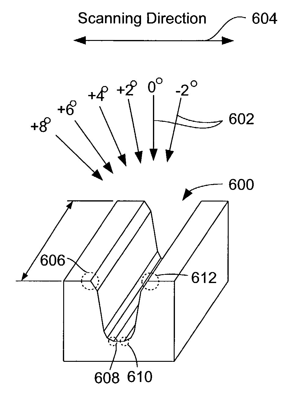
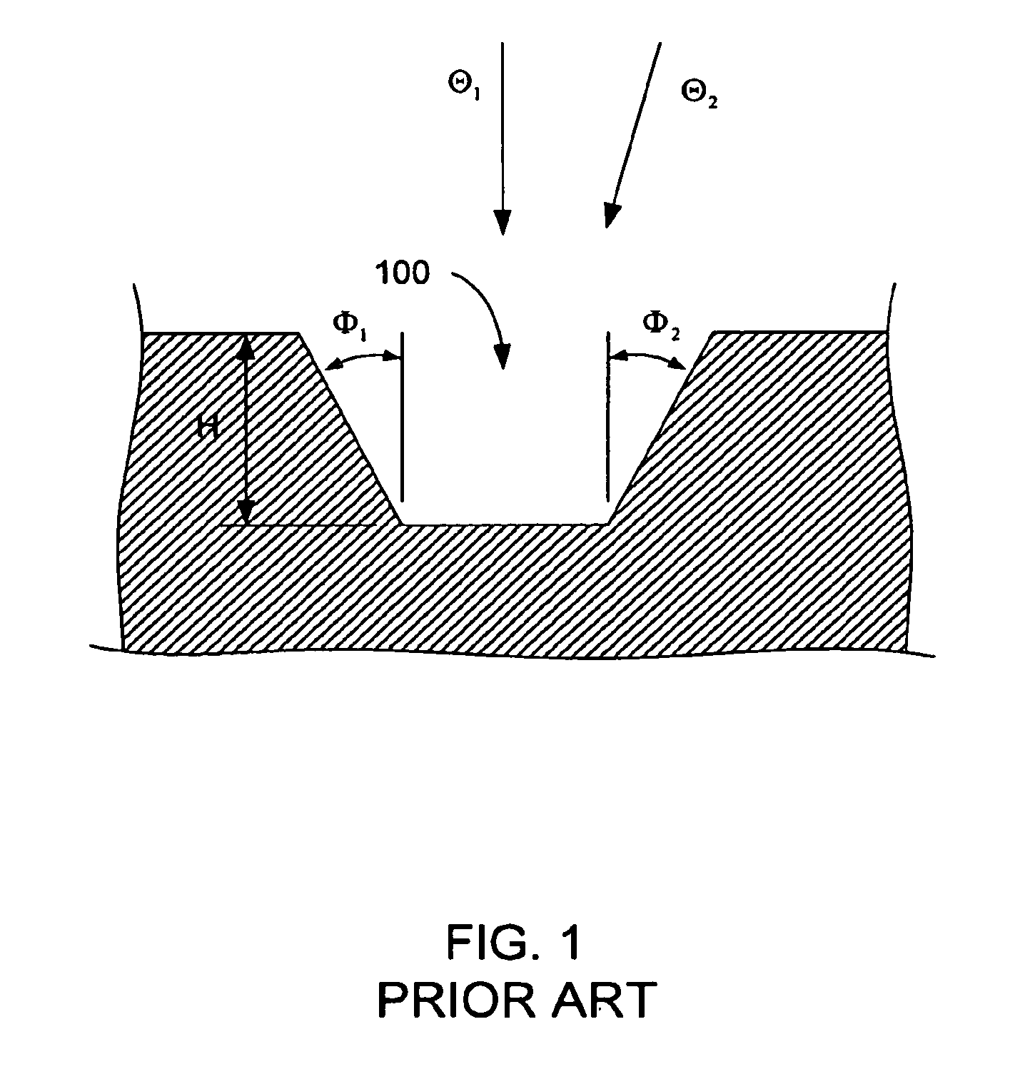
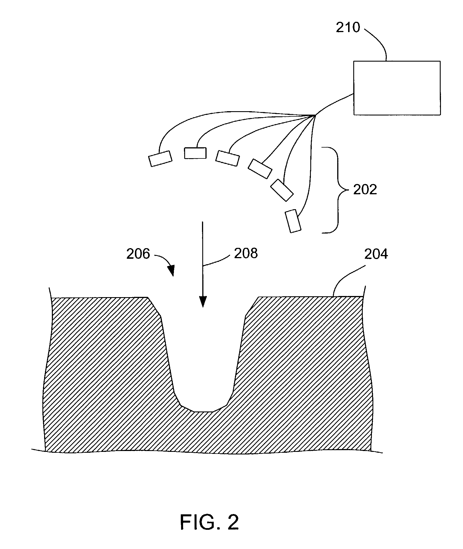
[0026]Generally, the present invention relates to a highly accurate technique for inspecting semiconductor devices. The inventive technique involves utilizing multiple sets of measurement data obtained by a scanning electron microscope (SEM) to determine the three-dimensional parameters of a semiconductor device. We define here a set of measurement data as an SEM image or scan. The SEM will collect each set of measu...


PUM


Abstract

A highly accurate technique for inspecting semiconductor devices is described. The technique involves utilizing multiple sets of measurement data obtained by a scanning electron microscope (SEM) to determine the dimensional parameters of a semiconductor device. The SEM collects each set of data from a different angular orientation with respect to the device. The dimensional parameters of the semiconductor device are determined by analyzing the relationship between the SEM inspection angle and the collected data sets. Various configurations of an SEM can be used to implement this invention. For instance an electron beam inspection system of the present invention can have at least two sets of deflectors for guiding the electron beam, a swiveling specimen stage, and/or a set of detectors set about the specimen at different angular orientations.

Description

CROSS REFERENCE TO RELATED APPLICATIONS[0001]This application claims priority of U.S. Provisional Patent Application No. 60 / 395,848, filed Jul. 11, 2002, which application is incorporated herein by reference in its entirety for all purposes.FIELD OF THE INVENTION[0002]The present invention relates generally to semiconductor inspection techniques, and more specifically to inspection techniques that utilize multiple sets of data gathered from different positions about a semiconductor specimen.BACKGROUND OF THE INVENTION[0003]The industry of semiconductor manufacturing involves highly complex techniques for integrating circuits within semiconductor materials. Due to the large scale of circuit integration and the decreasing size of semiconductor devices, the semiconductor manufacturing process is prone to processing defects. Inspection procedures are therefore critical to maintain quality control. Since the inspection techniques play an integral and significant part of the manufacturing...

Claims


Application Information

Patent Timeline
IPC IPC(8): G01N23/00G01N23/225G01Q20/00G01Q30/04G01Q30/02
CPCG01N23/2251H01J2237/226H01J2237/2611H01J2237/28
Inventor LORUSSO, GIAN FRANCESCOWATTS, ROBERT ANTHONYGUBBENS, ALEXANDER JOZEFHORDON, LAURENCE STUART
Owner KLA TENCOR TECH CORP
Why Eureka
Try Eureka