Arrangement of integrated circuits in a memory module

a memory module and integrated circuit technology, applied in the field of memory modules, can solve the problems of high heat generation, increased cost of non-standard integrated circuits, and high cost of micro-bga integrated circuits, and achieve the effect of reducing and increasing the cost of micro-bga connectors

Inactive Publication Date: 2005-08-16
NETLIST INC
View PDF74 Cites 151 Cited by
  • Summary
  • Abstract
  • Description
  • Claims
  • Application Information

AI Technical Summary

Problems solved by technology

Achieving the effective memory density on the printed circuit board has presented a substantial challenge to memory module manufacturers.
Use of non-standard integrated circuits, such as micro-BGA integrated circuits increases costs.
However, integrated circuits using micro-BGA connectors typically cost twice as much as comparable capacity TSOP integrated circuits.
However, the stacking of integrated circuits results in twice as much heat generation as with single layers of integrated circuits, with no corresponding increase in surface area.
Consequently, memory modules using stacked integrated circuits have substantial disadvantages over memory modules using a single layer of integrated circuits.
Operating at higher temperatures increases the incidence of bit failure.
Thermal fatigue and physical failure of the connections between the circuit board and the integrated circuit can result from ongoing heating and cooling cycles.

Method used


Image

  • Arrangement of integrated circuits in a memory module
  • Arrangement of integrated circuits in a memory module
  • Arrangement of integrated circuits in a memory module

Examples


Embodiment Construction

[0028]In the following description, reference is made to the accompanying drawings, which show, by way of illustration, specific embodiments in which the invention may be practiced. Numerous specific details of these embodiments are set forth in order to provide a thorough understanding of the invention. However, it will be obvious to one skilled in the art that the invention may be practiced without the specific details or with certain alternative components and methods to those described herein.

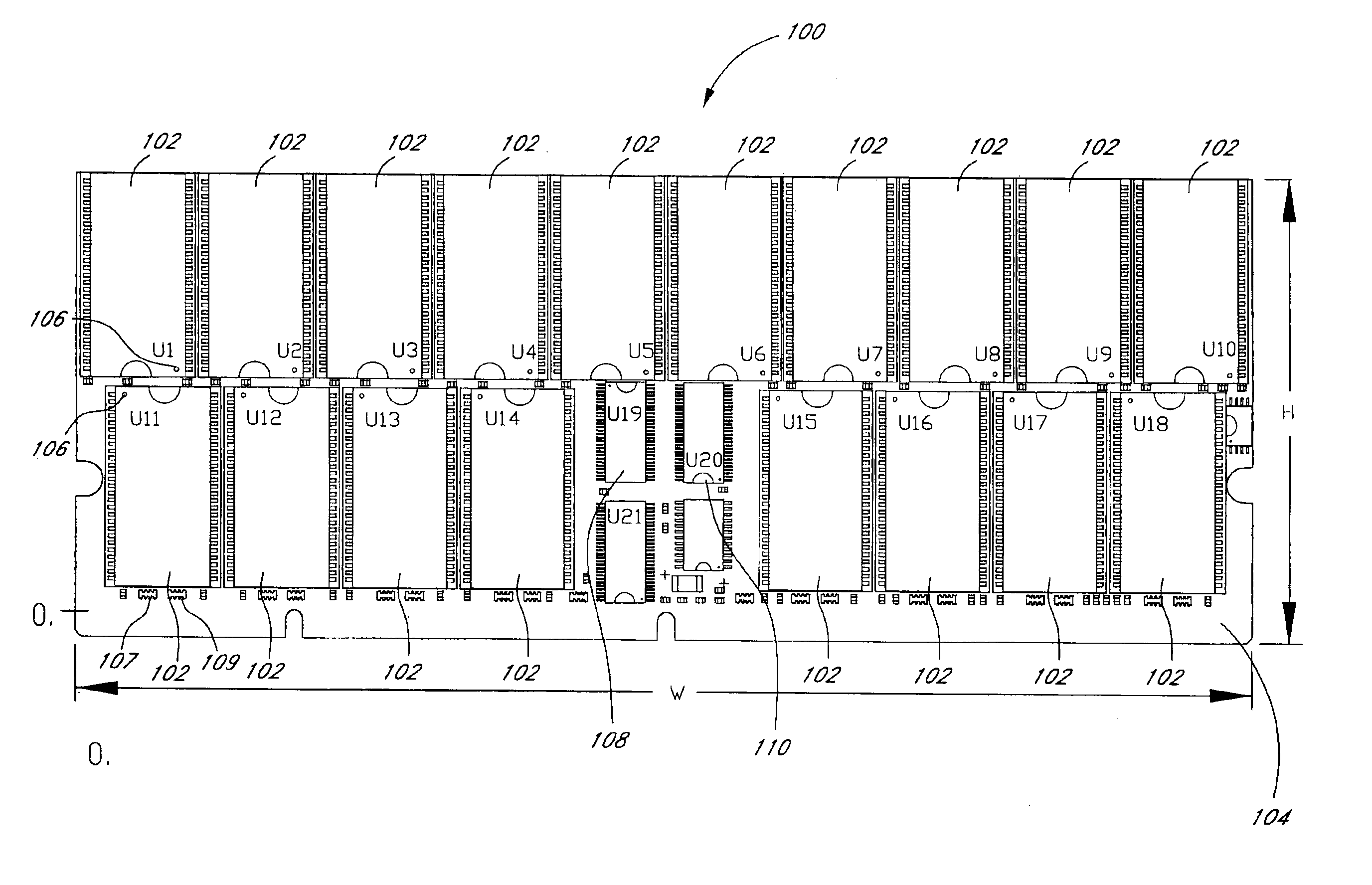
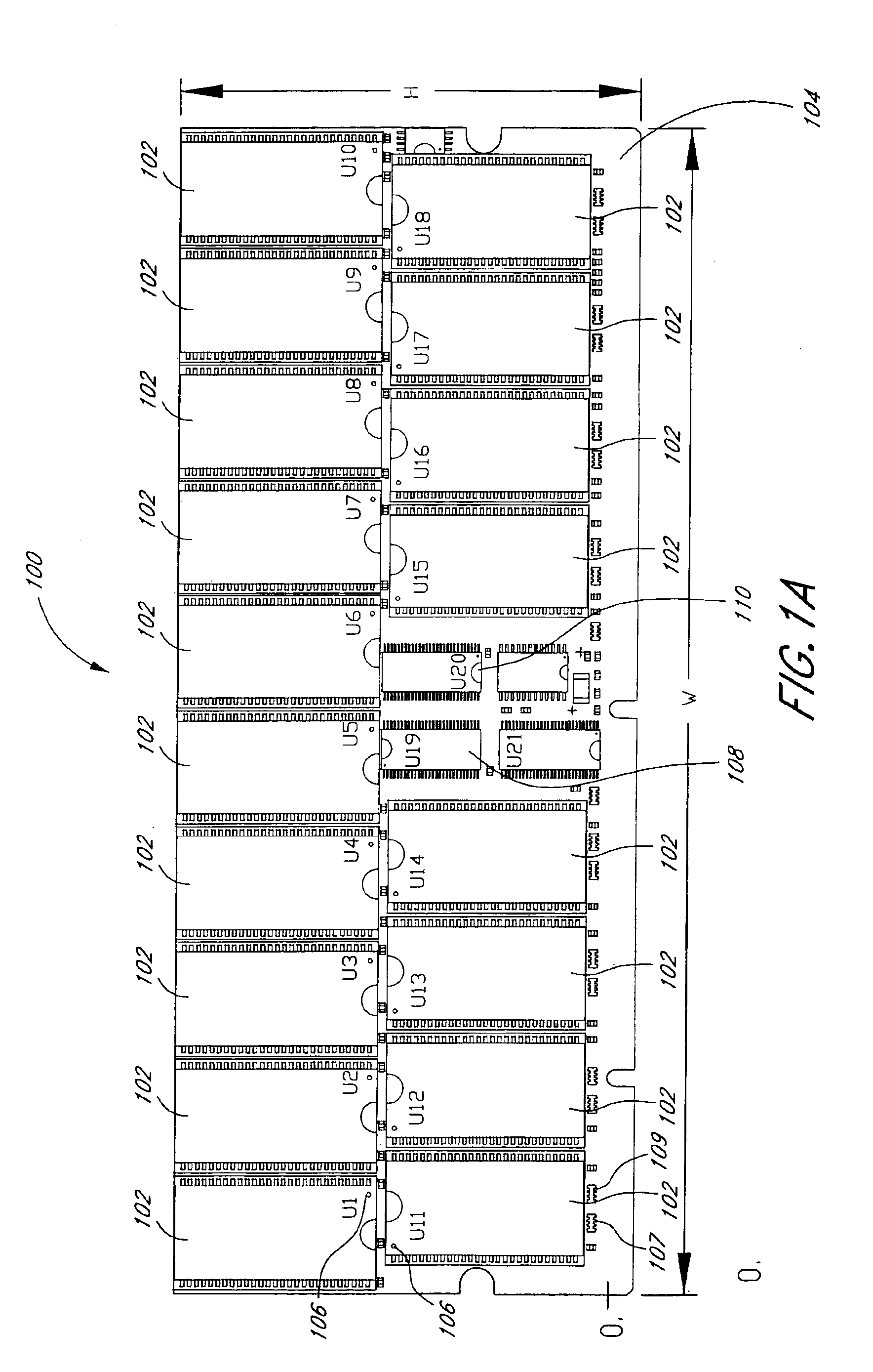
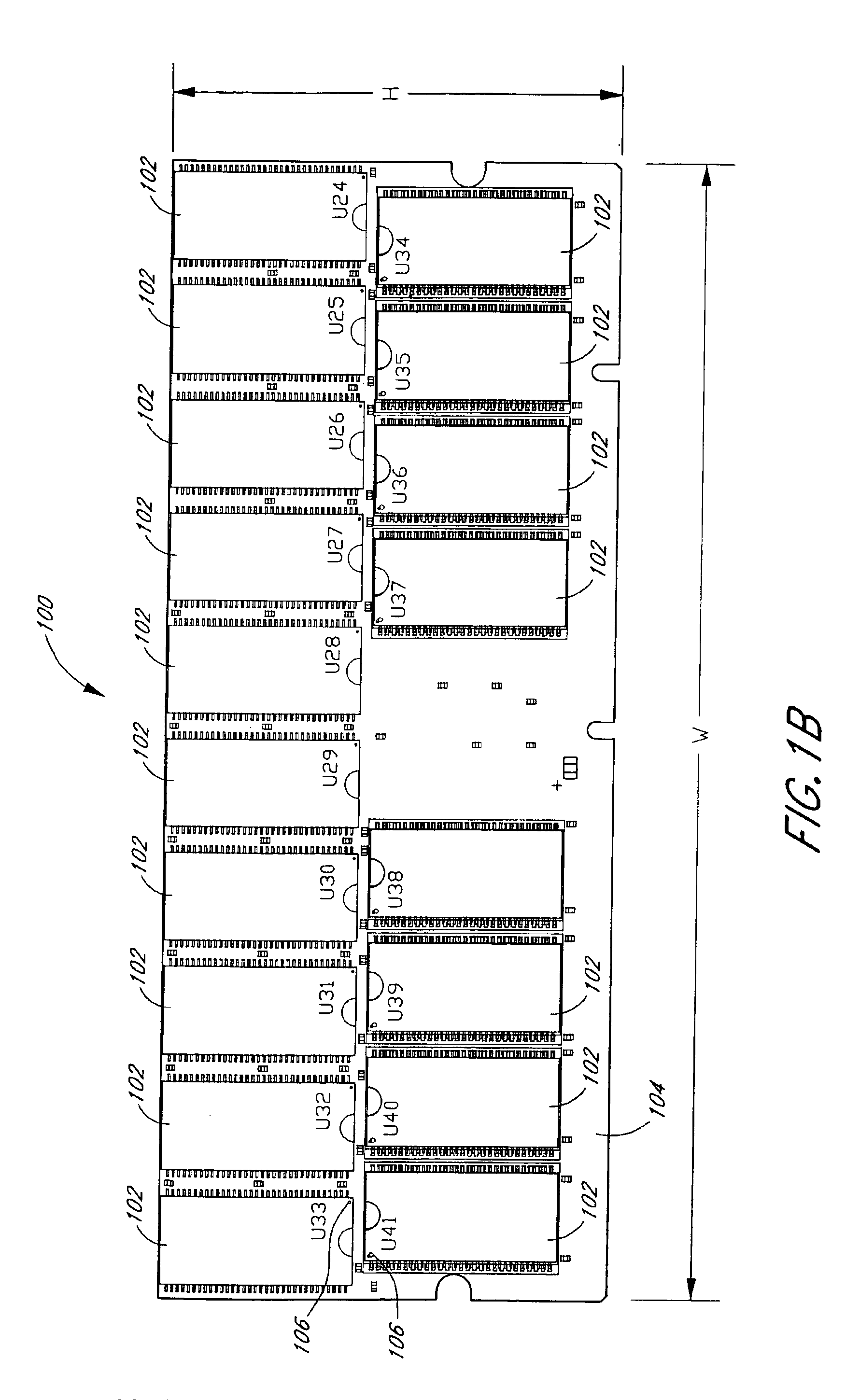
[0029]FIG. 1A illustrates the primary side of an embodiment of a memory module 100. The module 100 comprises two rows of memory integrated circuits 102 mounted onto a printed circuit board 104. The memory module 100 meets the timing standards for and is compatible with JEDEC requirements for a PC133 SDRAM module, but departs from the design guidelines contained in the PC133 design specification. In particular, the memory module 100 meets the timing and interface requirements of the PC133 st...


PUM


Abstract

Integrated circuits utilizing standard commercial packaging are arranged on a printed circuit board to allow the production of 1-Gigabyte and 2-Gigabyte capacity memory modules. A first row of integrated circuits is oriented in an opposite orientation to a second row of integrated circuits. The integrated circuits in a first half of the first row and in the corresponding half of the second row are connected via a signal trace to a first register. The integrated circuits in a second half of the first row and in the corresponding half of the second row are connected to a second register. Each register processes a non-contiguous subset of the bits in each data word.

Description

CLAIM OF PRIORITY[0001]This application is a divisional of U.S. patent application Ser. No. 10 / 094,512, filed Mar. 7, 2002, now U.S. Pat. No. 6,751,113, the disclosure of which is hereby incorporated in its entirety by reference herein.CROSS-REFERENCE TO CO-PENDING APPLICATIONS[0002]This application is related to U.S. patent application Ser. No. 10 / 674,240, filed Sep. 29, 2003, U.S. patent application Ser. No. 10 / 674,082, filed Sep. 29, 2003, and U.S. patent application Ser. No. 10 / 765,420, filed on Jan. 27, 2004, each of which is a divisional application of U.S. patent application Ser. No. 10 / 094,512, filed Mar. 7, 2002 now U.S. Pat. No. 6,751,113. This application is also related to U.S. patent application Ser. No. 10 / 769,469, filed on Jan. 29, 2004, which is a continuation-in-part of U.S. patent application Ser. No. 10 / 094,512, filed on Mar. 7, 2002, and to U.S. patent application Ser. No. 10 / 768,534, filed on Jan. 30, 2004, which is a continuation of U.S. patent application Ser....

Claims


Application Information

Patent Timeline
Patent Type & Authority Patents(United States)
IPC IPC(8): G11C5/00H05K1/18H05K1/02
CPCH05K1/181H05K1/0266H05K2201/09409H05K2201/09709H05K2201/10689Y02P70/50
Inventor BHAKTA, JAYESH R.PAULEY, JR., ROBERT S.
Owner NETLIST INC
Why Eureka
Try Eureka