FeRAM semiconductor memory

Active Publication Date: 2005-08-16
STMICROELECTRONICS SRL
View PDF10 Cites 11 Cited by
  • Summary
  • Abstract
  • Description
  • Claims
  • Application Information

AI Technical Summary

Problems solved by technology

The disadvantage of such solution resides in that the semiconductor chip area is occupied by the charge pumps that include capacitors, diodes, a generator of phases for driving the capacitors and an output voltage regulator.
Another drawback is the power consumption of these circuits; in order to limit such power consumption, it is necessary to implement charge pump turn-off and turn-on schemes, that, however, contribute to increasing the area occupied.
Also, this solution has the disadvantage of involving a great waste of area.
Nevertheless, this solution poses limitations to the design of the memory cells arrangement.

Method used


Image

  • FeRAM semiconductor memory
  • FeRAM semiconductor memory
  • FeRAM semiconductor memory

Examples


Embodiment Construction

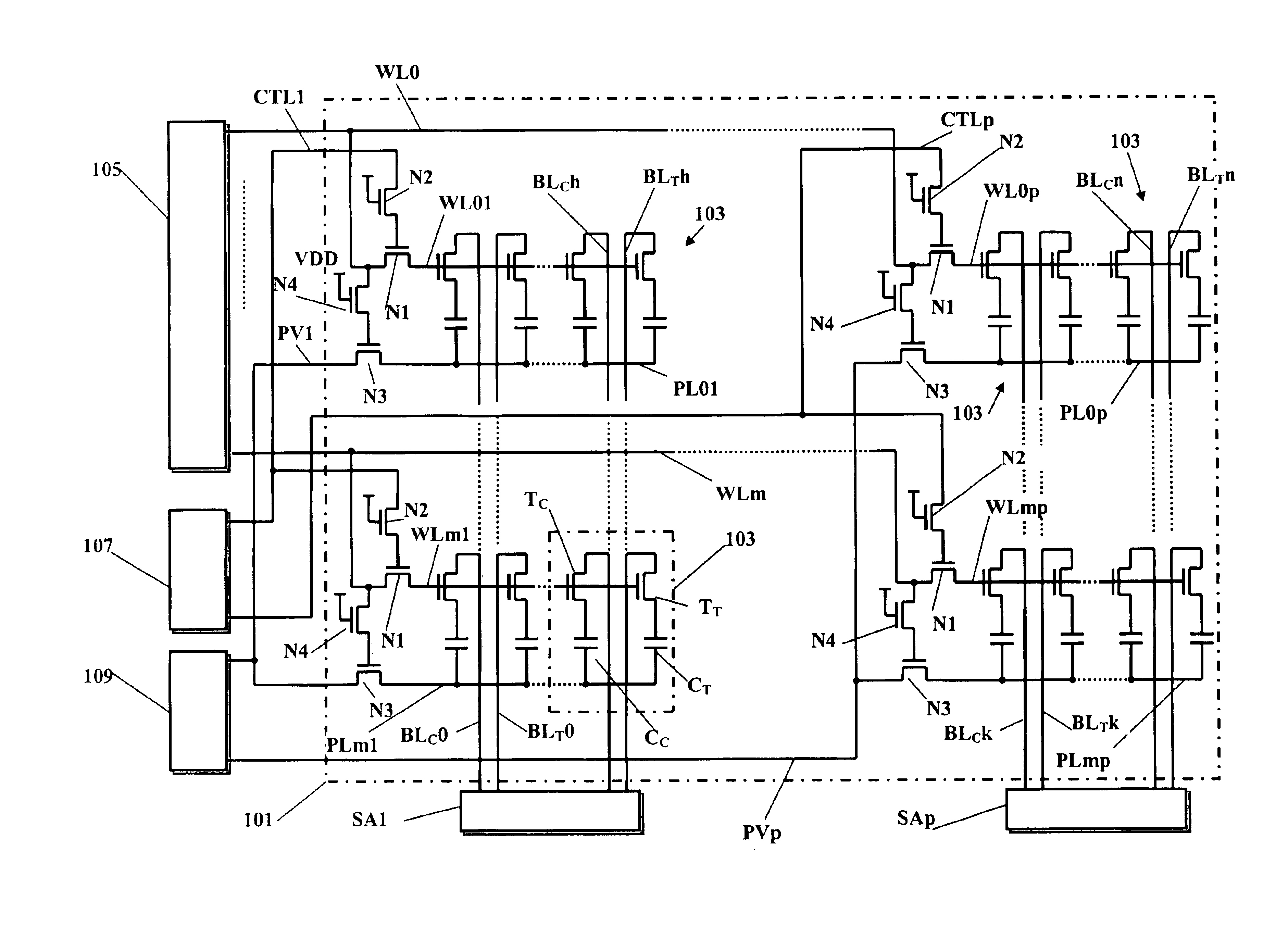
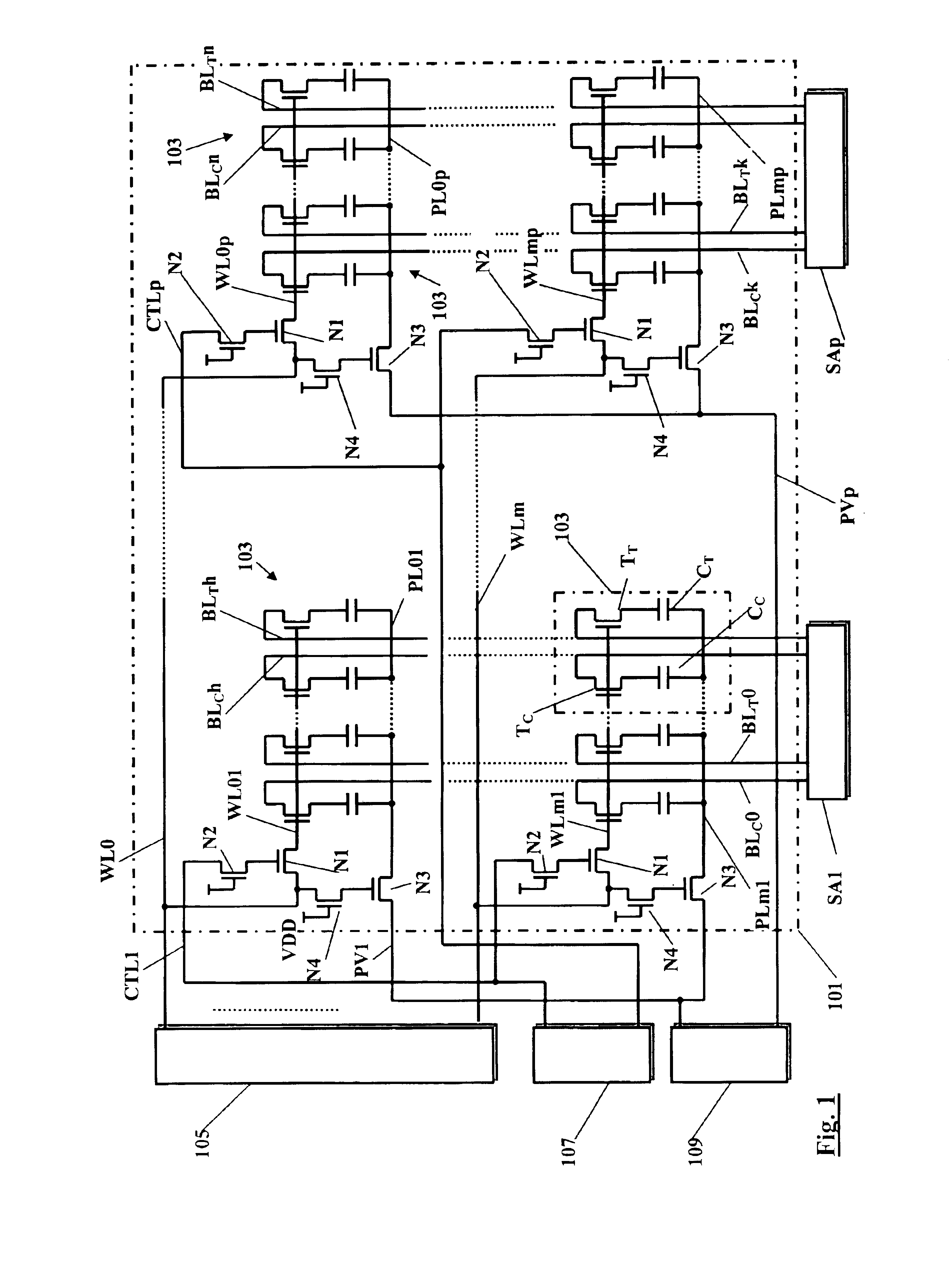
[0037]Making reference to FIG. 1, an FeRAM ferroelectric memory according to an embodiment of the present invention is schematically depicted. In particular, the FeRAM memory shown in FIG. 1 is of the “2T2C” type.

[0038]The memory includes a bidimensional arrangement or matrix 101 of memory units 103, each one adapted to store a binary unit of information (“bit”).

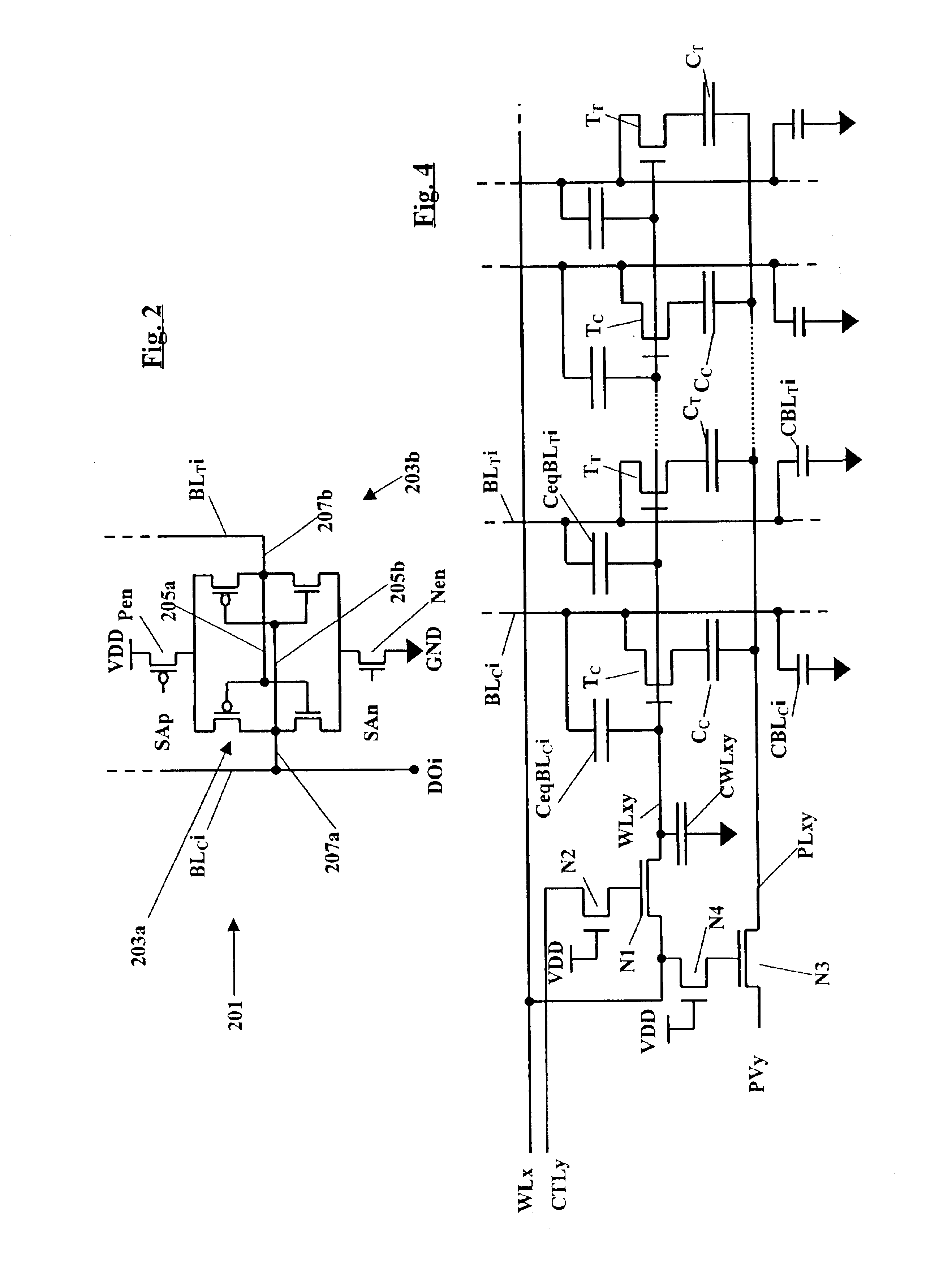
[0039]Each memory unit includes two FeRAM memory cells. Each FeRAM memory cell is formed of a selection transistor TC, TT, for instance, an N-channel MOSFET; in series to the source of the selection transistor TC, TT, a storage capacitor Cc, CT is provided, whose dielectric comprises a ferroelectric material.

[0040]The memory units 103 are arranged in a plurality of rows and a plurality of columns. A respective word line WL0-WLm corresponds to each row of the matrix. A respective pair of bit lines BLC0, BLT0-BLCn, BLTn corresponds to each column of the matrix.

[0041]The memory units 103 that belong to a same matrix column have...


PUM


Abstract

A ferroelectric semiconductor memory includes an arrangement of memory units comprising at least one row of memory units. The memory units of the at least one row are associated with a respective word line of the arrangement. The arrangement of memory unit includes a plurality of local word lines branching off from the word line associated with the at least one row, each local word line being connected to a respective group of memory units of the line. Selective connection means allow to selectively connect one of the local word lines to the respective word line. The arrangement of memory units further includes a plurality of local plate biasing lines, each one associated with the memory units of a respective group of memory units, for selectively driving the memory units of the respective groups.

Description

PRIORITY CLAIM[0001]This application claims priority from Italian patent application No. MI2002A000793, filed Apr. 15, 2002, which is incorporated herein by reference.TECHNICAL FIELD[0002]The present invention relates generally to the field of semiconductor memory devices, and particularly to non-volatile memories. More specifically, the invention concerns a ferroelectric non-volatile memory of the type referred to as FeRAM.BACKGROUND OF THE INVENTION[0003]Ferroelectric, non-volatile memories have memory cells consisting of a selection transistor, or access transistor, and, connected in series to the selection transistor, a storage capacitor whose dielectric is formed by a film of ferroelectric material.[0004]Applying an electric field of sufficient intensity to the storage capacitor, the ferroelectric material becomes polarized in the direction of the electric field, and, thus, the polarization achieved is also maintained after the electric field is removed. If, at a later time, an...

Claims


Application Information

Patent Timeline
IPC IPC(8): G11C11/22G11C7/00G11C7/18
CPCG11C7/18G11C11/22G11C2211/4013
Inventor SBERNO, GIAMPIEROTORRISI, SALVATOREDEMANGE, NICOLAS
Owner STMICROELECTRONICS SRL
Why Eureka
Try Eureka