
Method for manufacturing of a vertical light emitting device structure

a manufacturing method and technology of light-emitting devices, applied in semiconductor/solid-state device manufacturing, semiconductor devices, electrical equipment, etc., can solve the problems of insufficient lighting facilities, difficult to meet the more practical use of leds in human life, etc., to reduce costs, simplify manufacturing process, and facilitate sliced

Inactive Publication Date: 2005-08-23
SEMILEDS OPTOELECTRONICS CO LTD
View PDF13 Cites 27 Cited by
  • Summary
  • Abstract
  • Description
  • Claims
  • Application Information

AI Technical Summary

Benefits of technology

"The present invention provides a new LED structure that has a larger lighting area and illumination. The LED has a simplified manufacturing process and a larger lighting area, which can replace a smaller LED for a fixed brightness and reduce the cost needed. The LED also has a higher thermal conductive coefficient, making it suitable for high power applications. The LED structure includes a substrate unit with a weak spot, a multi-layer epitaxial structure, a metal reflector, a conductive substrate, and an LED vertical structure. The LED vertical structure includes an upper surface with a p-electrode and a bottom side with an n-electrode. The used substrate for epitaxial layers can be sapphire, but other materials can also be used. The wire bonding operation needs to be executed only once, reducing cost for packaging and deficiency. The LED structure with Si as the conductive substrate is well suitable for high power applications."

Problems solved by technology

However, brightness has always been the biggest issue in the field, which has been challenging the more practical uses of LEDs in human living utilization.
However, the results are not satisfactory enough in quest of the LED-based lighting facilities, one of the reasons is that the n-electrode is in the way of the produced light when the light emits out of the device.
In the n-electrode's view, the light-emitting device structure is not completely a pure vertical structure, which leads to a reduction of the lighting surface of the device.
However, the n-electrode is a source of limiting the lighting area according to the state of the art, also described above, and hence one of the reasons limiting the luminous efficiency of the LED since the n-electrode may hinder the lighting area on the LED, which may be readily known through FIG. 15, through which the desired light is emitted.
Therefore, the illumination produced by the LED has long been not enhanced with respect to the limited lighting area of the LED.

Method used


Image

  • Method for manufacturing of a vertical light emitting device structure
  • Method for manufacturing of a vertical light emitting device structure
  • Method for manufacturing of a vertical light emitting device structure

Examples


second embodiment

[0037]Referring to FIG. 6 showing the present invention, it is constructed by further forming over the p+-GaN based semiconductor layer 27 of the multi-layer epitaxial structure 2 in the preferred embodiment a doped metal oxide 28 which is light transparent to a light emitted from the device structure and has a suitable thickness, i.e., the emitted light may penetrate therethrough and serves as a window layer. The doped metal oxide layer 28 may be doped ZnO, a metal oxide doped with ZnO, InxZn1−xO, SnxZn1−xO and InxSnyZn1−x−y, etc., wherein 0≦X≦1, 0≦Y≦1 and 0≦X+Y≦1. The dopant added in the doped metal oxide layer 28 may be a Group-V element, such as Al. Besides, a doped metal oxide with a refractive index of at least 1.5, an n-type metal oxide, a p-type metal oxide or a rare earth element doped metal oxide may also be the choice. The thickness of the doped metal oxide depends on the actual material used therefor, and may be 50 Å to 50 μm for ZnO doped material. The p-electrode 40 is...

third embodiment

[0038]Referring to FIG. 7 illustrating the present invention, a p-type distributed Bragg Reflector (p-DBR) 26 may be further formed between the InGaN / GaN MQW active layer 22 and the p+-GaN based semiconductor layer 27 for the structure 2 in the preferred embodiment and comprises a p-AlGaN / GaN DBR, with a reflectance of 50-80%. In this case, between the metal reflector 31 and the p-type DBR 26 forms a resonant cavity, and the produced light may also excite the MQW active layer 22 in addition to the applied electric bias.

[0039]Referring to FIG. 8 illustrating a fourth embodiment of the present invention, a metal oxide 28 is further formed over the p+-GaN based semiconductor layer 27 therein, wherein the metal oxide 28 has a suitable thickness and light transparency, and is used as a window layer. The description about the metal oxide 28 has been given in the second embodiment in the present invention and will be omitted herein. The p-electrode 40 is finally disposed over an upper surf...

fifth embodiment

[0040]Referring to FIG. 9 illustrating a fifth vertical device structure embodiment according to the present invention, a multi-layer epitaxial structure 2, a metal reflector 31, a conductive substrate 33, a p-electrode 40 and an n-electrode 50 are comprised. The multi-layer epitaxial structure 2 comprises an n-GaN based semiconductor layer 21, a second MQW active layer 23, a second n-GaN based layer 24, a first MQW active layer 25, a p-DBR 26 and a contact layer 27 in sequence. The n-GaN based layer 21 may be doped n-GaN, for example, one doped with Si for electricity conduction purpose, and has a thickness of 2-6 μm. The second MQW active layer 23 may be InGaN / GaN. The second n-GaN layer 24 may be doped n-GaN, for example, one doped with Si for electricity conduction purpose, and has a thickness of 2-6 μm. The first MQW active layer 25 may be InGaN / GaN. The p-AlGaN / GaN DBR has a reflectance of 50-80%. The contact layer 27 is a p-GaN based semiconductor layer, which may be such as ...


PUM

PropertyMeasurementUnit
thickaaaaaaaaaa
thicknessaaaaaaaaaa
thicknessaaaaaaaaaa

Abstract

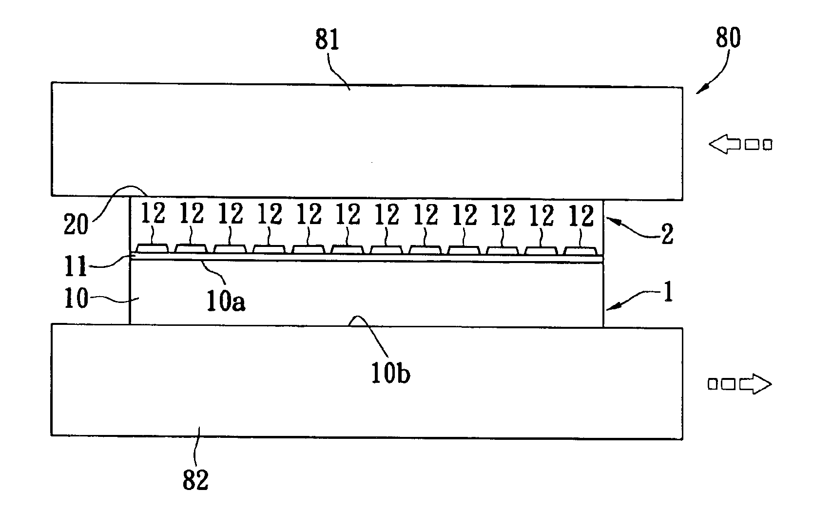
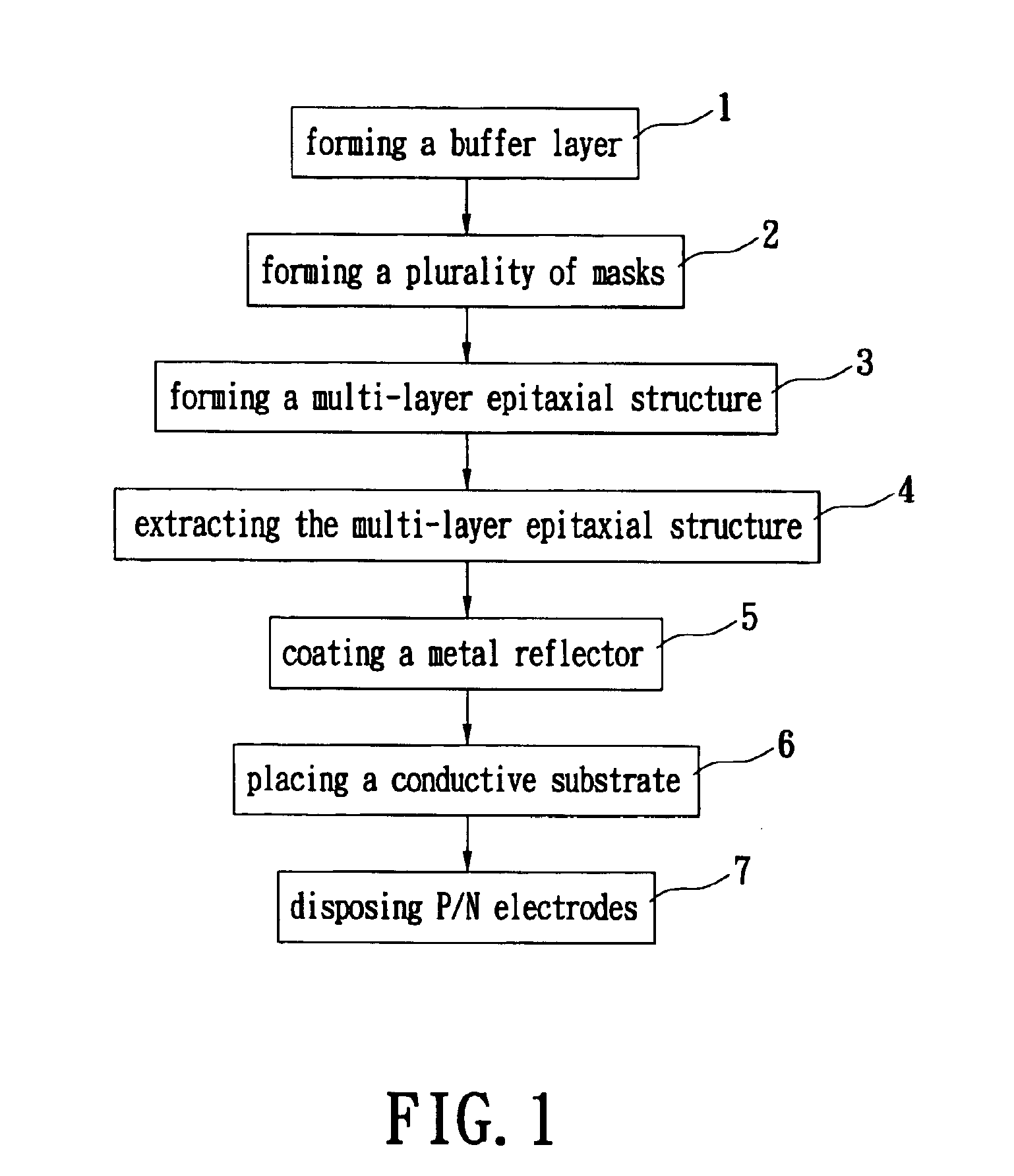
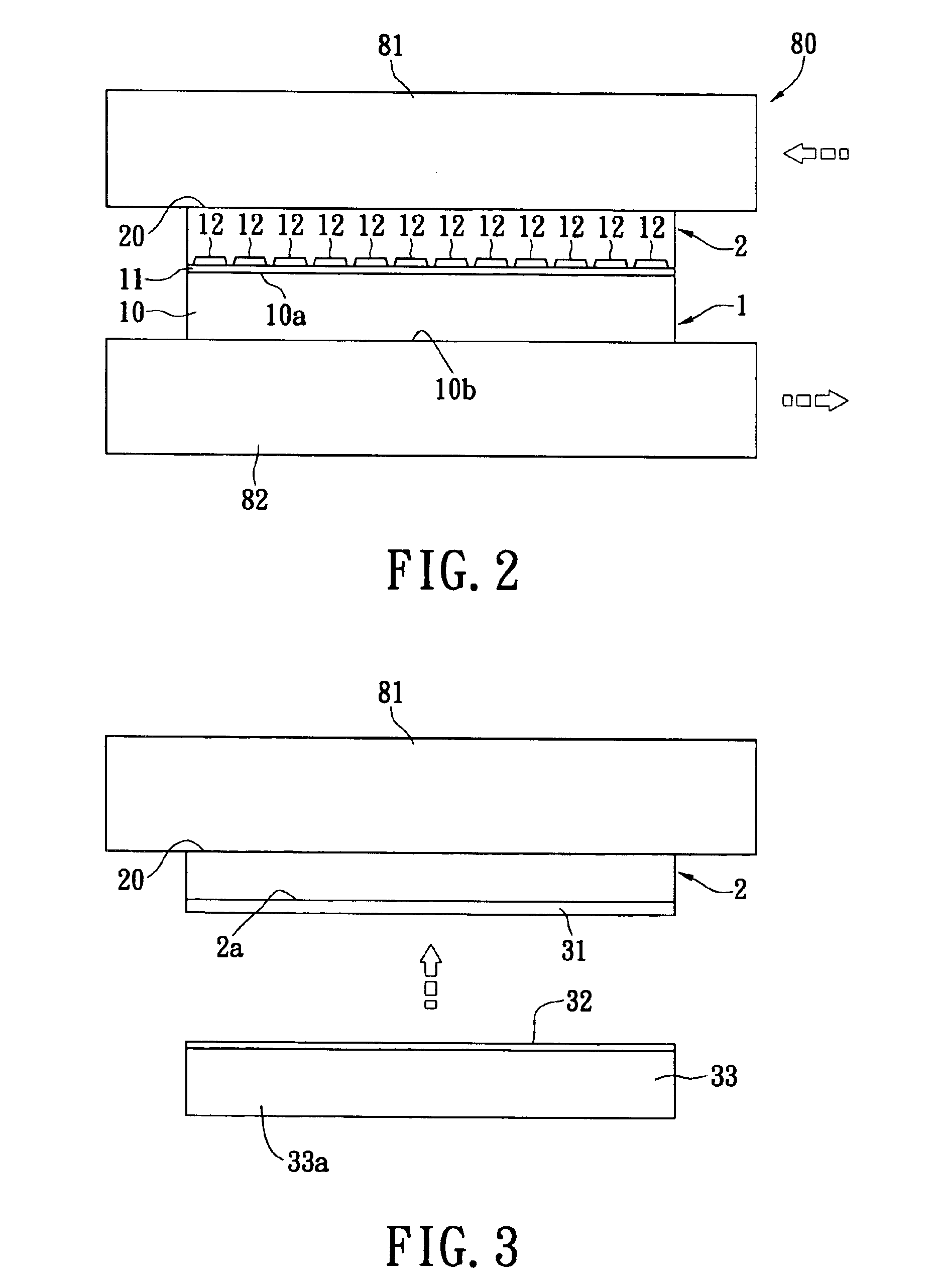
Disclosed are a vertical GaN based light-emitting device (LED) structure and the manufacturing method thereof. In the structure and the corresponding method, a substrate unit having a mask is used to form a multi-layer epitaxial structure and the substrate and the multi-layer epitaxial structure are separated at the mask. After the multi-layer epitaxial structure is extracted, a metal reflector may be disposed thereunder. Next, a conductive substrate is bonded to the metal reflector. Next, an upper surface of the multi-layer structure is disposed with a p-electrode and a bottom side of the conductive substrate with an n-electrode whereby an vertical LED structure is formed.

Description

BACKGROUND OF THE INVENTION[0001]1. Field of the Invention[0002]The present invention is related to a light-emitting device (LED) structure of and the manufacturing method thereof, and particularly to, a vertical GaN-based LED structure and the manufacturing method thereof. More particularly, the vertical LED structure is a completely vertical structure and has a larger lighting area and the corresponding manufacturing method may be simplified at the same time.[0003]2. Description of Related Art[0004]Light-emitting diodes (LEDs) have been widely known as useful lighting facilities and expected to become the most important and efficient ones. As we see, they have been founded useful in some important applications, such as communications and other areas, such as mobile phone and some appliances. Recently, there is a trend that further introducing LEDs to ordinary human living utilization, such as large panels, traffic lights and lighting facilities and the perspective thereof are look...

Claims


Application Information

Patent Timeline
Patent Type & Authority Patents(United States)
IPC IPC(8): H01L33/00H01L33/06H01L33/10H01L33/12H01L33/32H01L33/40H01L33/42
CPCH01L33/405H01L33/0079H01L33/0093
Inventor HON, SCHANG-JING
Owner SEMILEDS OPTOELECTRONICS CO LTD
Learn More