DC offset cancellation circuit, differential amplification circuit with DC offset cancellation circuit, photo-electric pulse conversion circuit, pulse shaping circuit, and pulse generation circuit

Inactive Publication Date: 2005-08-23
FUJITSU MICROELECTRONICS LTD
View PDF7 Cites 17 Cited by
  • Summary
  • Abstract
  • Description
  • Claims
  • Application Information

AI Technical Summary

Benefits of technology

[0067]Since the seventh signal that rises at the rise timing of the optical pulse signal and the eighth signal that rises at the fall timing of the optical pulse signal are separately obtained as described above, it is possible to obtain the non-inversion shaped electrical pulse signal or the inversion shaped electrical pulse signal that sharply rises or falls at the rise timing (the second timing) or the fall tim

Problems solved by technology

As a result, there may arise a problem that AC components gradually accumulate, the output signals are distorted, and the dynamic range of the

Method used


Image

  • DC offset cancellation circuit, differential amplification circuit with DC offset cancellation circuit, photo-electric pulse conversion circuit, pulse shaping circuit, and pulse generation circuit
  • DC offset cancellation circuit, differential amplification circuit with DC offset cancellation circuit, photo-electric pulse conversion circuit, pulse shaping circuit, and pulse generation circuit
  • DC offset cancellation circuit, differential amplification circuit with DC offset cancellation circuit, photo-electric pulse conversion circuit, pulse shaping circuit, and pulse generation circuit

Examples


Example

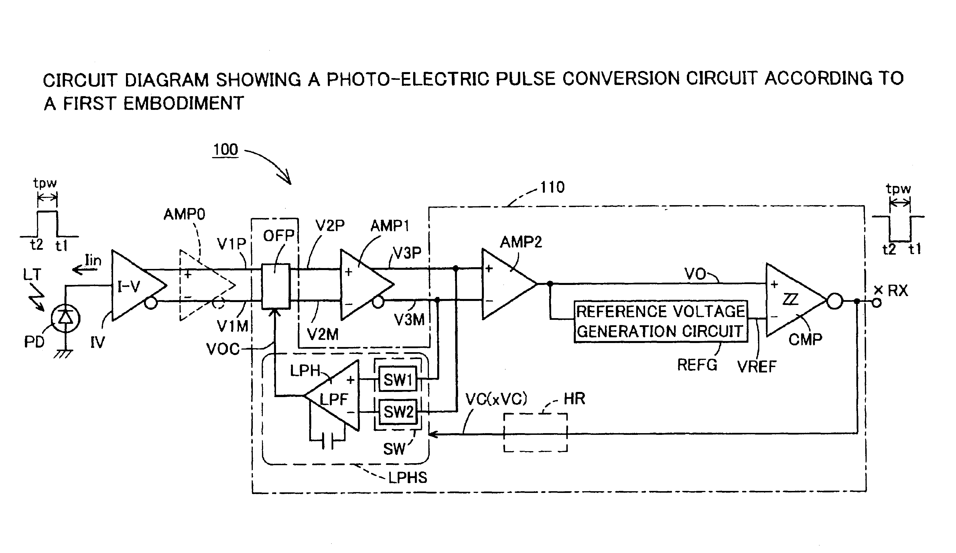
[0113]A first embodiment of the present invention will be explained with reference to FIGS. 1 through 6. A photo-electric pulse conversion circuit 100 according to the first embodiment shown in FIG. 1 is used in a receiving circuit in IrDA or other optical communications. Namely, the photo-electric pulse conversion circuit converts an optical pulse signal LT entering a photodiode PD to a corresponding electrical pulse signal xRX while retaining a pulse tpw. It thereafter performs other types of necessary processing in a demodulator circuit or other circuits at later stages.

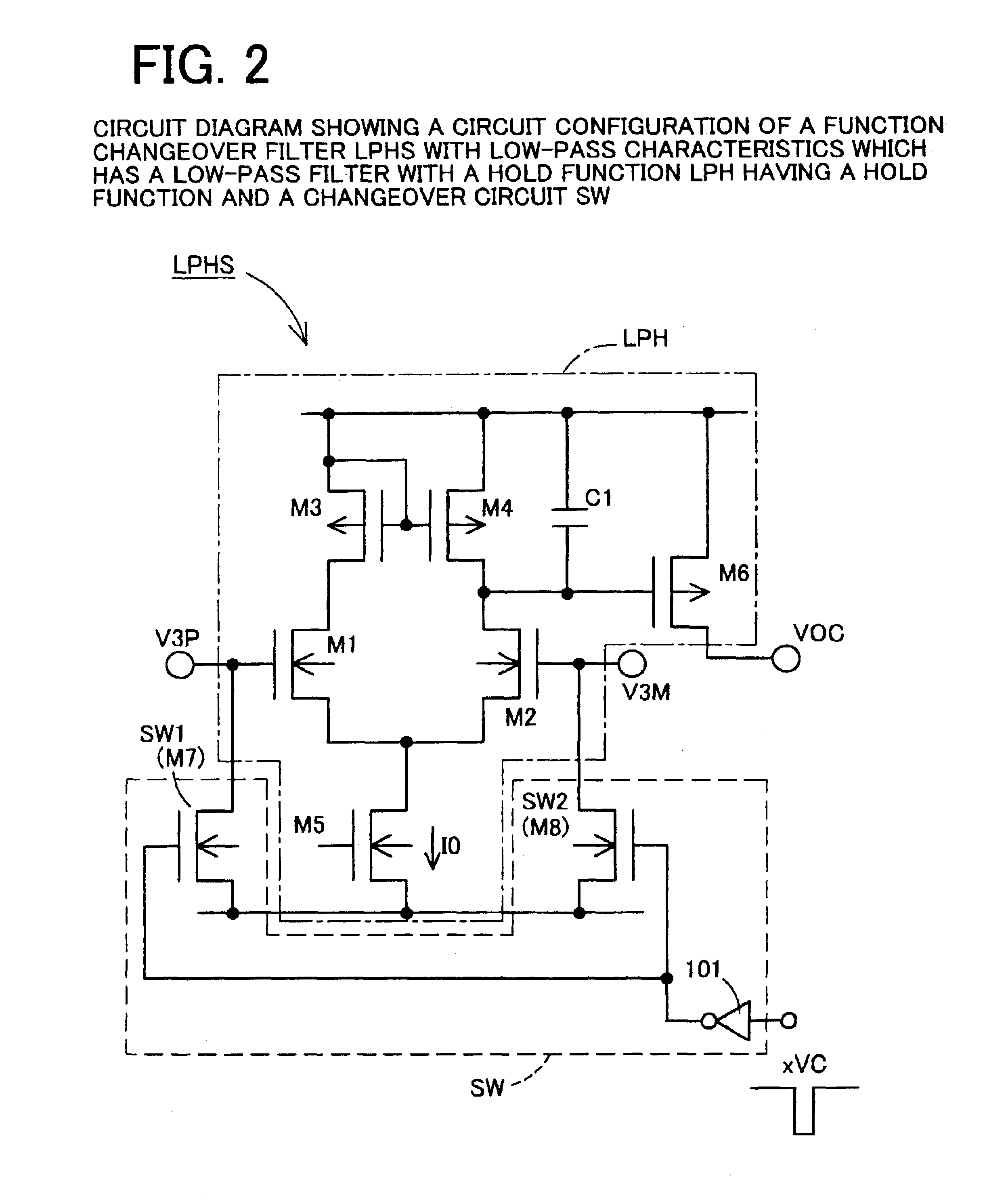
[0114]The photo-electric pulse conversion circuit 100 has nearly the same configuration as the above-mentioned photo-electric pulse conversion circuit 10, except that a DC offset cancellation circuit 110 for canceling a DC offset voltage occurring in a first differential amplification circuit AMP1 is configured differently.

[0115]In the same manner as in the photo-electric pulse conversion circuit 10, therefore, wh...

Example

[0134]A second embodiment of the invention will be explained with reference to FIGS. 7 through 9. A photo-electric pulse conversion circuit 200 according to the second embodiment shown in FIG. 7 has nearly the same configuration as the above-mentioned photo-electric pulse conversion circuit 20, except for the configuration of a DC offset cancellation circuit 210 for canceling a DC offset voltage occurring in a differential amplification circuit AMP.

[0135]Therefore, an optical pulse signal LT that rises at a second timing t2 and falls at a first timing t1 is received by a photodiode PD to obtain a current signal Iin also in the photo-electric pulse conversion circuit 200. Then, a differentiating I-V conversion circuit DIV is used to convert the current signal Iin to a pair of complementary differential voltage signals VD1P, VD1M having waveforms similar to a differentiated waveform of the current signal Iin and outputs the voltage signals. The differential voltage signals VD1P, VD1M ...

Example

[0167]A third embodiment of the invention will be explained with reference to FIGS. 13 through 18. A photo-electric pulse conversion circuit 300 according to the third embodiment shown in FIG. 13 has nearly the same configuration in a first half portion thereof as the above-mentioned photo-electric pulse conversion circuit 30. However, the circuit is different in that a pulse shaping circuit 310 includes an offset-added signal generation circuit OFS that generates a signal to which an offset voltage has been added, two comparison circuits CMP1, CMP2, and a logic processing circuit LGC in stages subsequent to a differentiating differential amplification circuit DAMP.

[0168]Therefore, an optical pulse signal LT that rises at a second timing t2 and falls at a first timing t1 is received by a photodiode PD to obtain a current signal Iin also in this photo-electric pulse conversion circuit 300. The current signal Iin is thereafter converted to a corresponding voltage signal V1 and the res...


PUM


Abstract

A DC offset cancellation circuit that is capable of canceling a DC offset voltage occurring between a pair of differential output signals of a differential amplification circuit, while preventing a signal waveform from being distorted due to accumulation of AC components and a photo-electric pulse conversion circuit that is capable of generating an electrical pulse signal that accurately reproduces a rise timing and a fall timing of an optical pulse signal by canceling the DC offset voltage are provided. A photo-electric pulse conversion circuit is provided with a photodiode, an I-V conversion circuit, a first differential amplification circuit having a DC offset cancellation circuit, a second differential amplification circuit, a reference voltage generation circuit, and a comparison circuit. The DC offset cancellation circuit uses a changeover circuit to change a state of a low-pass filter with a hold function in synchronization with an inversion electrical pulse signal, and performs a negative feedback of a filtered signal which is generated by subjecting third differential signals to low-pass filtration or a hold filtered signal which is a filtered signal held during changeover.

Description

[0001]This is a division of application Ser. No. 10 / 041,593, filed Jan. 10, 2002, now U.S. Pat. No. 6,549,054.BACKGROUND OF THE INVENTION[0002]1. Field of the Invention[0003]The present invention relates to a DC offset cancellation circuit that cancels a DC offset voltage occurring between a pair of complementary differential output signals outputted from a differential amplification circuit, a differential amplification circuit with a DC offset cancellation circuit, and a photo-electric pulse conversion circuit that uses the differential amplification circuit capable of DC offset cancellation to convert an optical pulse signal to a corresponding electrical pulse.[0004]Alternatively, it relates to a pulse shaping circuit that generates a shaped pulse signal whose logic changes in a manner similar to a rise and a fall of a base square-wave pulse signal, a pulse generation circuit that uses this pulse shaping circuit, and a photo-electric pulse conversion circuit that uses the pulse s...

Claims


Application Information

Patent Timeline
IPC IPC(8): H03K5/13H03F3/08H03F3/45H03F3/04H03K5/007H03K5/08H04B10/152H04B10/158H03K5/153G01J1/44H03K5/003H03K9/08H04B10/2507H04B10/40H04B10/50H04B10/60
CPCH03F3/087H03F3/45098H03F3/45179H03F3/45183H03F3/45475H03F3/45753H03F3/45771H03F3/45973H03F3/45977H03F3/45982H03F3/45995H03K5/003H03K5/007H03K5/08H03K5/13H03K5/153H04B10/6933H03F2203/45521
Inventor ONO, AKIHIKO
Owner FUJITSU MICROELECTRONICS LTD
Why Eureka
Try Eureka