Confocal wafer-inspection system

a wafer-inspection and optical technology, applied in the field of three-dimensional objects, can solve the problems of low accuracy in height measurement, differences in height of various bumps,

Inactive Publication Date: 2005-08-23
CAMTEK LTD
View PDF8 Cites 40 Cited by
  • Summary
  • Abstract
  • Description
  • Claims
  • Application Information

AI Technical Summary

Problems solved by technology

Actually, there are differences between the heights of the various bumps, as a result of the production process.
Various systems for wafer-inspection are known and the main disadvantage of all those systems is a low accuracy in height measurement.

Method used


Image

  • Confocal wafer-inspection system
  • Confocal wafer-inspection system
  • Confocal wafer-inspection system

Examples


Embodiment Construction

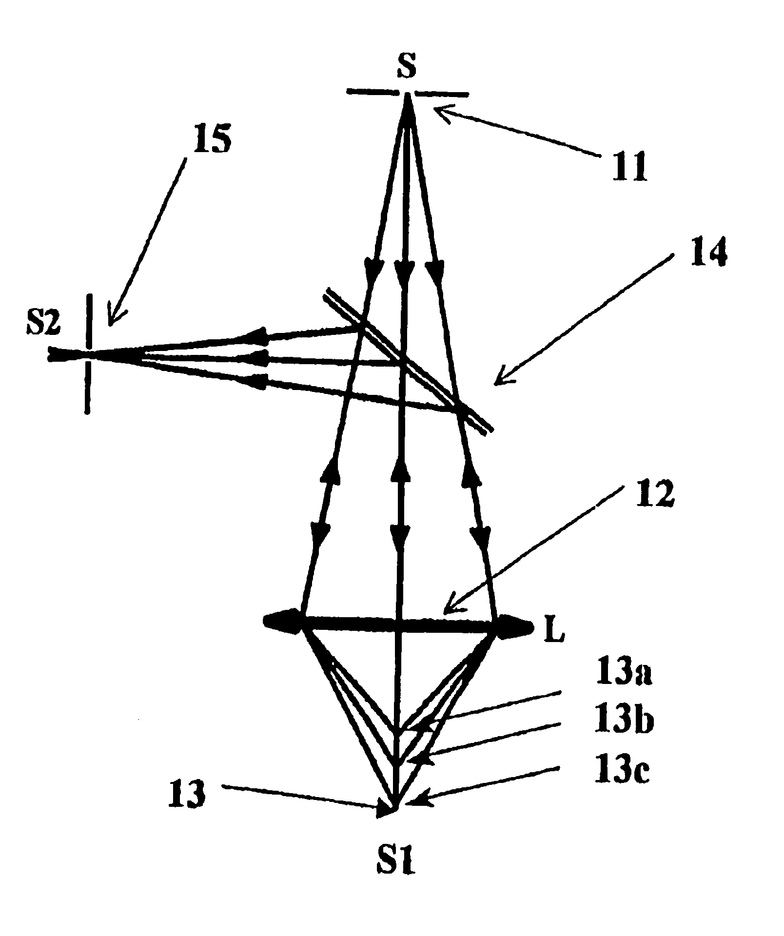
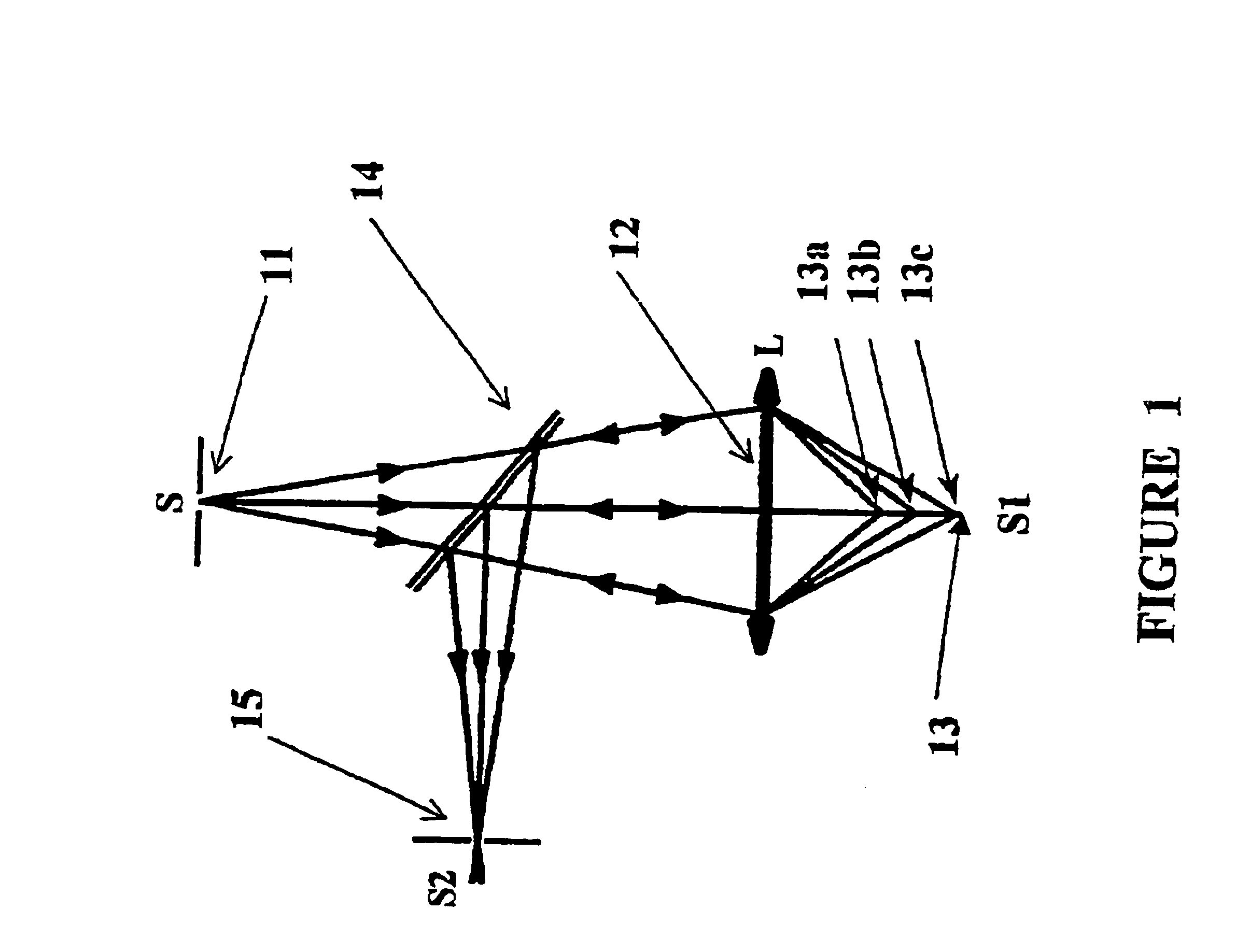
[0044]The present invention is a confocal wafer-inspection system.

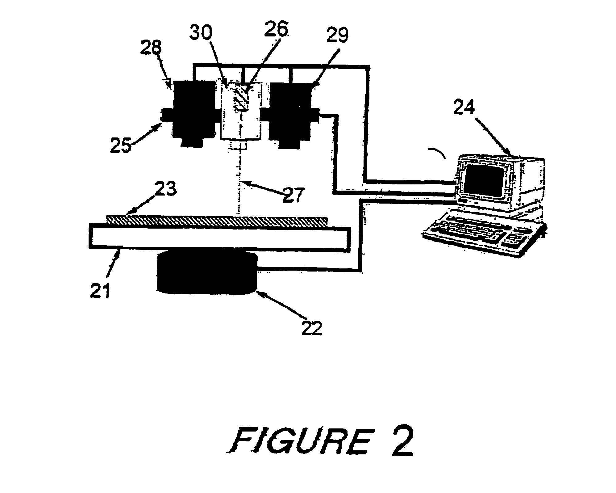
[0045]The system has a table with two vertical degrees of freedom enables a movement means to move the table in XY axis. A wafer is laying on the table and a confocal height measurement system, a microscope, a first camera and a second camera are installed perpendicular to the table, held by a horizontal movement means. A computer controls the vertical movement means and the horizontal movement means. The microscope and the confocal height measurement system are aimed to the same point.

[0046]An inspected wafer lies down on the table. The computer controls the movement of the table by the movement means, enables each point of the wafer surface being under the aim point. The microscope observes the wafer's surface and the first camera photograph the view and the image is transferred to the computer, which display the image on the screen. The image is used by an operator of the system to overview the surface and enables ...


PUM

PropertyMeasurementUnit
confocal chromatic height measurementaaaaaaaaaa
surface heightaaaaaaaaaa
heightaaaaaaaaaa

Abstract

A confocal wafer inspection system including: (a) a table to carry a wafer for inspection, the table having two vertical degrees of freedom to enable XY axis movements; (b) a movement device for moving the table along the degrees of freedom; (c) a confocal height measurement system, perpendicular to the table, for measuring the range to a point on a surface of the wafer and for enabling to recognize changes in surface altitude while the wafer moves with the table; and (d) a computer operative for: (i) holding a bumps map of the wafer; (ii) controlling the movement device; (iii) moving the table so that the measuring point of the confocal height measurement system crosses each bump of the wafer; (iv) storing a height profile of each bump; (v) comparing the height profiles or checking each height profile according to predetermined criteria or both; and (vi) enabling a results output. The invention also relates to a method for confocal wafer inspection.

Description

[0001]This application is a Continuation of PCT / IL02 / 00841 filed Oct. 21, 2002, the contents of which are incorporated herein by reference.FIELD OF THE INVENTION[0002]The present invention relates to the field of checking the height of small objects, and more specifically, of three-dimensional objects by using height measurement techniques.BACKGROUND OF THE INVENTION[0003]A “bump” is a three-dimensional shape (half sphere or rectangular) salient, made of solder or gold located on the face of a microelectronic chip. The bump exists in some chips and substitutes as leads by means of which the component is connected to the printed circuit when the bumps are soldered to the board. The bump shape is usually a half ball alike. A chip can contain a large number of bumps, which should be of the same height in order to connect all of them to the board at the same time. Actually, there are differences between the heights of the various bumps, as a result of the production process. Only small ...

Claims


Application Information

Patent Timeline
Patent Type & Authority Patents(United States)
IPC IPC(8): G01B11/24G01B11/06G01B11/02G02B21/00G01N21/88G01N21/95H01L21/60H01L21/66
CPCG01B11/026G01B11/0608G01B11/24G01N21/9501G02B21/0024G02B21/0028G02B21/006G01B2210/50
Inventor GEFFEN, MICHAELLEVI, YAKI
Owner CAMTEK LTD
Why Eureka
Try Eureka