Method of forming a shallow junction

a junction and shallow technology, applied in the direction of semiconductor devices, electrical equipment, transistors, etc., can solve the problems of shallow source/drain extension junctions, poor junction profiles, and devices

Inactive Publication Date: 2005-08-30
INTEL CORP
View PDF2 Cites 42 Cited by
  • Summary
  • Abstract
  • Description
  • Claims
  • Application Information

AI Technical Summary

Problems solved by technology

The defects 108 can create several problems for a device.
The defects 113 enhance dopant diffusion resulting in a deeper source/drain extension junction and poor junction profile.
The

Method used


Image

  • Method of forming a shallow junction
  • Method of forming a shallow junction
  • Method of forming a shallow junction

Examples


Embodiment Construction

[0018]Exemplary embodiments are described with reference to specific configurations and techniques. Those of ordinary skill in the art will appreciate the various changes and modifications to be made while remaining within the scope of the appended claims. Additionally, well known elements, devices, components, circuits, process steps and the like are not set forth in detail.

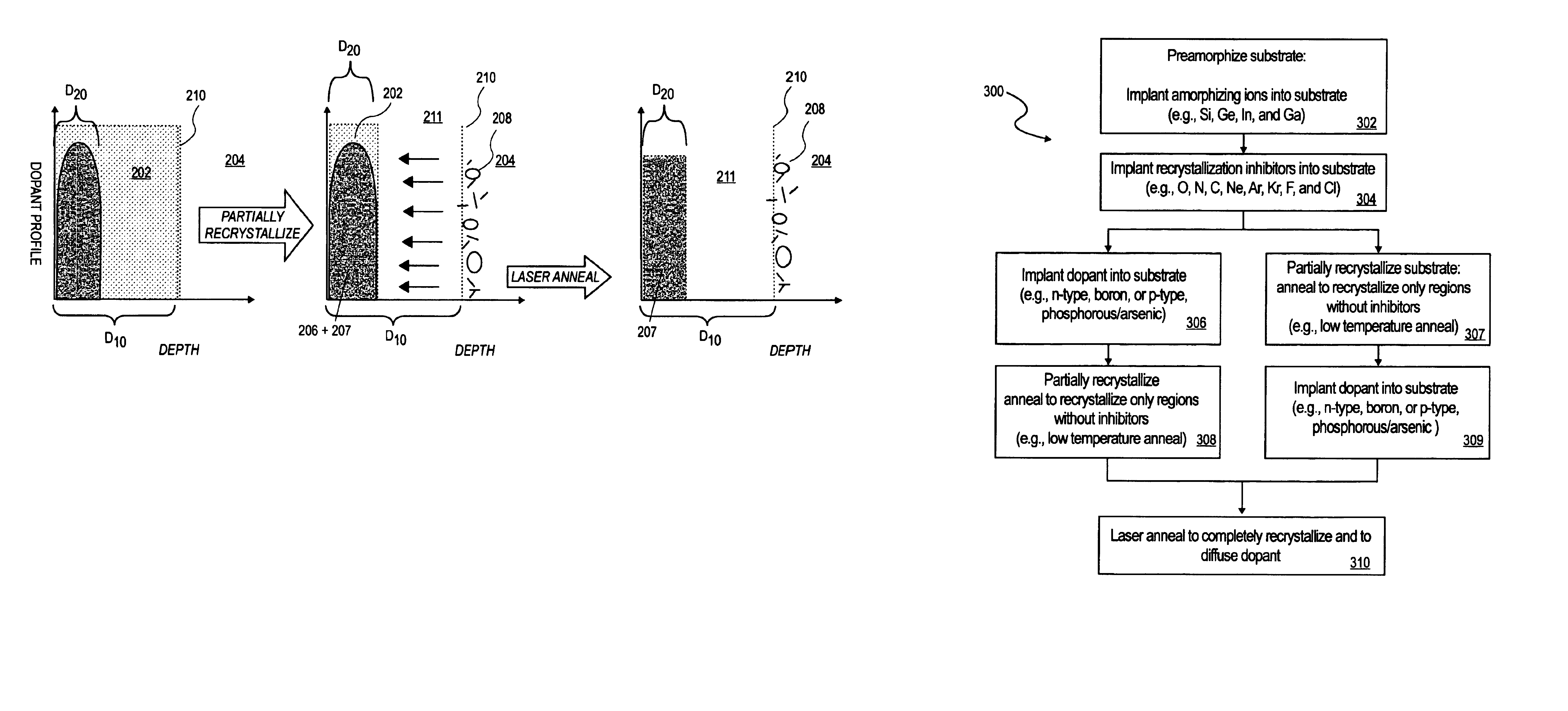
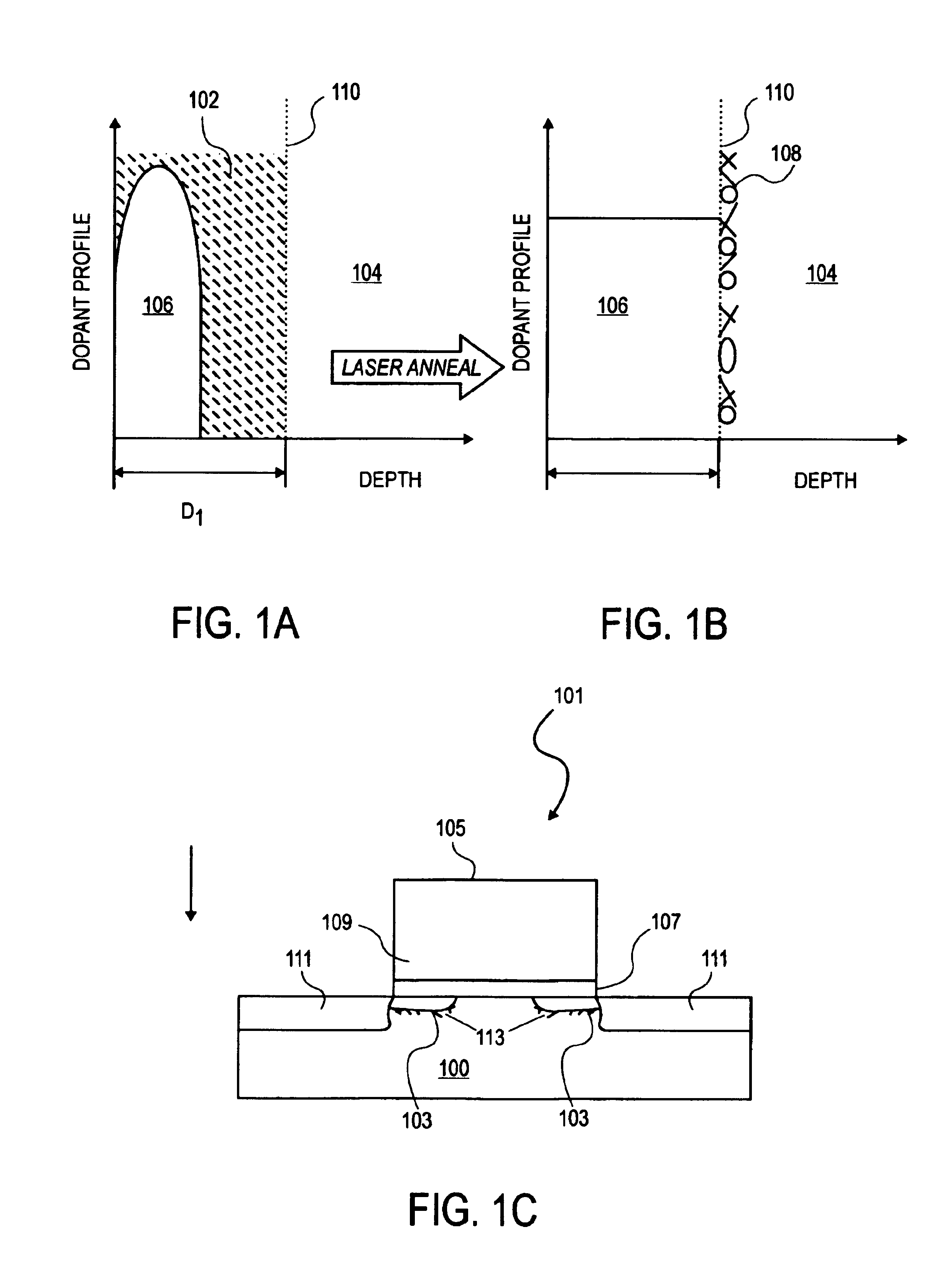
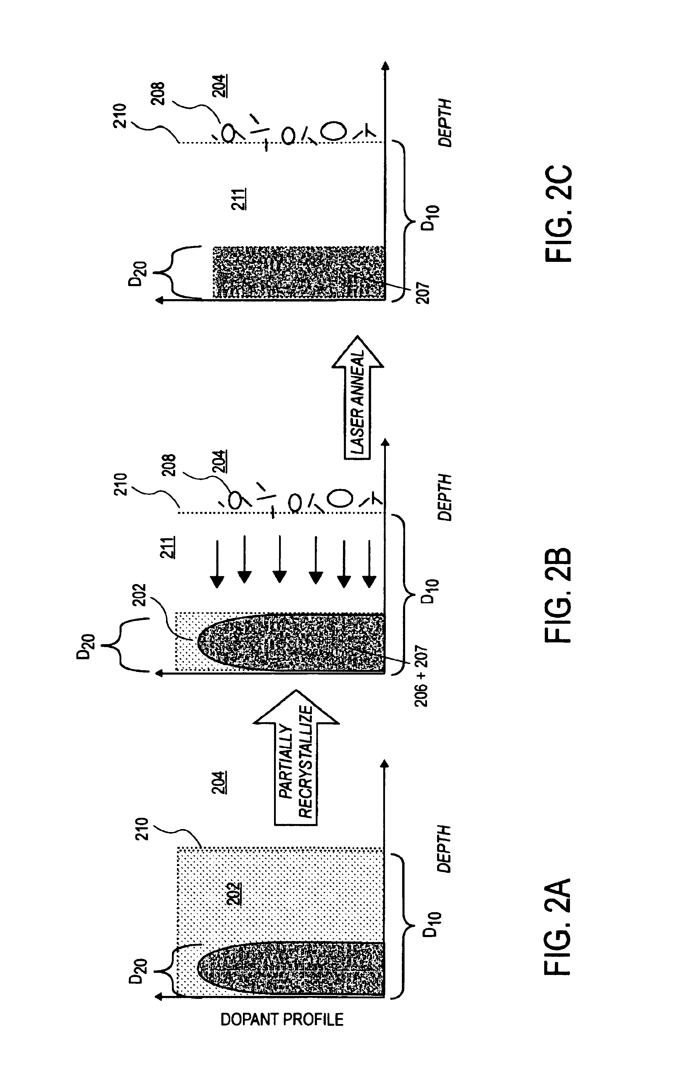
[0019]From the discussion above, an improved method for making a shallow junction is desired and will be advantageous to the advancement of microelectronic devices. For example, a method of making a shallow junction that is substantially defect-free is needed. In some embodiment, a substantially defect-free shallow junction refers to a shallow junction that is formed not in close proximity with EOR dislocations or other defects or that is formed in an area, which does not have EOR dislocations. As mentioned above, EOR dislocations often result from preamorphizing and recrystallizing a semiconductor substrate.

[00...


PUM


Abstract

A method of forming a shallow junction in a semiconductor substrate is disclosed. The method of one embodiment comprises preamorphizing a first region of a semiconductor substrate to a first depth and implanting recrystallization inhibitors into a second region of the semiconductor substrate. The second region is a part of the first region and has a second depth. Next, a dopant is implanted into a third region of the semiconductor substrate with the third region being a part of the second region and a first annealing is performed to selectively recrystallize the first region that has no recrystallization inhibitors. Next, a second annealing is performed to recrystallize the second region and diffuse the dopant within the second region.

Description

BACKGROUND[0001]1. Field[0002]Microelectronics fabrication, including a method of forming a shallow junction.[0003]2. Description of the Related Art[0004]Advances in semiconductor devices such as Complimentary Metal Oxide Semiconductor (CMOS) devices rely on the miniaturization of the devices. Smaller devices typically equate to faster switching times, which lead to speedier and better performance. Miniaturization of the devices involves scaling down various vertical and horizontal dimensions in the device structure. For example, the thickness of the ion implanted source / drain junction of a p-type or an n-type transistor is scaled down with a corresponding scaled increase in the substrate channel doping.[0005]For devices with a critical gate dimension in the submicron level, e.g., lesser than or equal to 0.1 μm, a shallow junction is required. Additionally, a source / drain extension junction with an abrupt profile slope is required.[0006]The formation of source / drain extension juncti...

Claims


Application Information

Patent Timeline
IPC IPC(8): H01L21/265H01L21/02H01L21/336H01L21/268H01L21/324H01L29/78H01L29/66
CPCH01L21/26506H01L21/26513H01L21/26586H01L21/268H01L21/324H01L29/6659H01L29/6656H01L29/7833H01L21/26593
Inventor KEYS, PATRICK H.CEA, STEPHEN M.
Owner INTEL CORP
Why Eureka
Try Eureka