Apparatus and method for testing electronic component

a technology for electronic components and apparatuses, which is applied in the manufacture of measuring leads/probes, instruments, capacitors, etc., can solve the problems of inability to measure the characteristics of electronic components with reduced size, the inability to use this testing apparatus to simultaneously measure, and the inability to measure the size of electronic components disclosed in patent document 1. achieve the effect of reducing the size of electronic components and easy and fast measuremen

Active Publication Date: 2005-08-30
MURATA MFG CO LTD
View PDF5 Cites 2 Cited by
  • Summary
  • Abstract
  • Description
  • Claims
  • Application Information

AI Technical Summary

Benefits of technology

[0013]In order to overcome the problems described above, preferred embodiments of the present invention provide an apparatus and a method for testing an electronic component such that various characteristics of electronic components, including capacitance, that cannot be measured when one of the electrodes is shared by a plurality of electronic components, are easily and quickly measured by general-purpose probes, even if the size of the electronic components is reduced.

Problems solved by technology

However, recent size reduction of electronic components causes some problems.
That is, characteristics of an electronic component with reduced size cannot be measured.
Since the conductive plates 63 arranged under the cavities 62 are shared by a plurality of electronic components, however, use of this testing apparatus is limited to measurement of particular characteristics, such as insulation resistance, that can be measured even when one of the electrodes of the electronic component is shared with other electronic components.
In other words, the apparatus for testing electronic components disclosed in Patent Document 1 cannot be used to simultaneously measure characteristics, such as capacitance, that cannot be measured when one of the electrodes of the electronic component is shared with other electronic components.

Method used


Image

  • Apparatus and method for testing electronic component
  • Apparatus and method for testing electronic component
  • Apparatus and method for testing electronic component

Examples


Embodiment Construction

[0028]Preferred embodiments of the present invention will now be described with reference to the drawings.

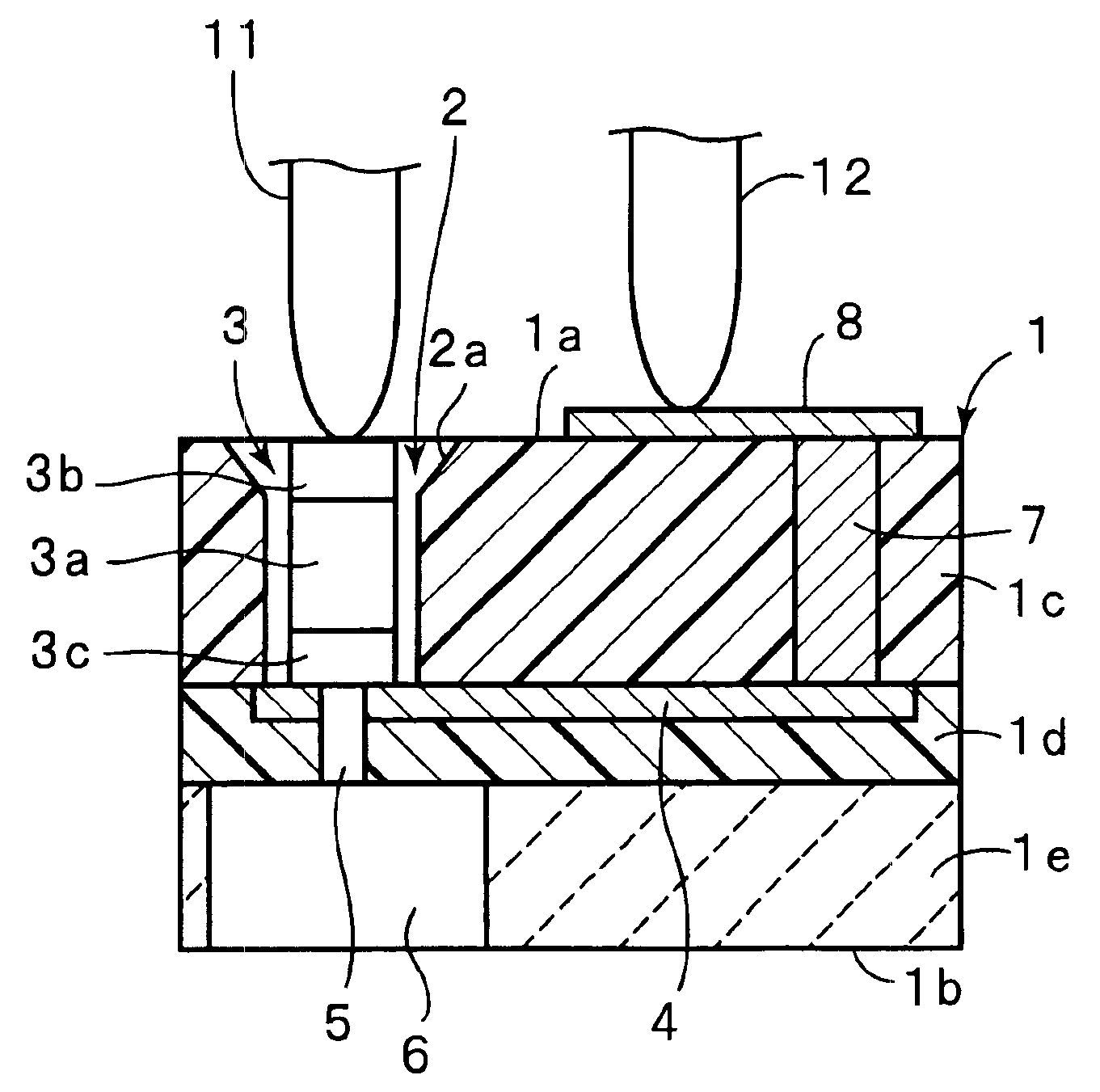
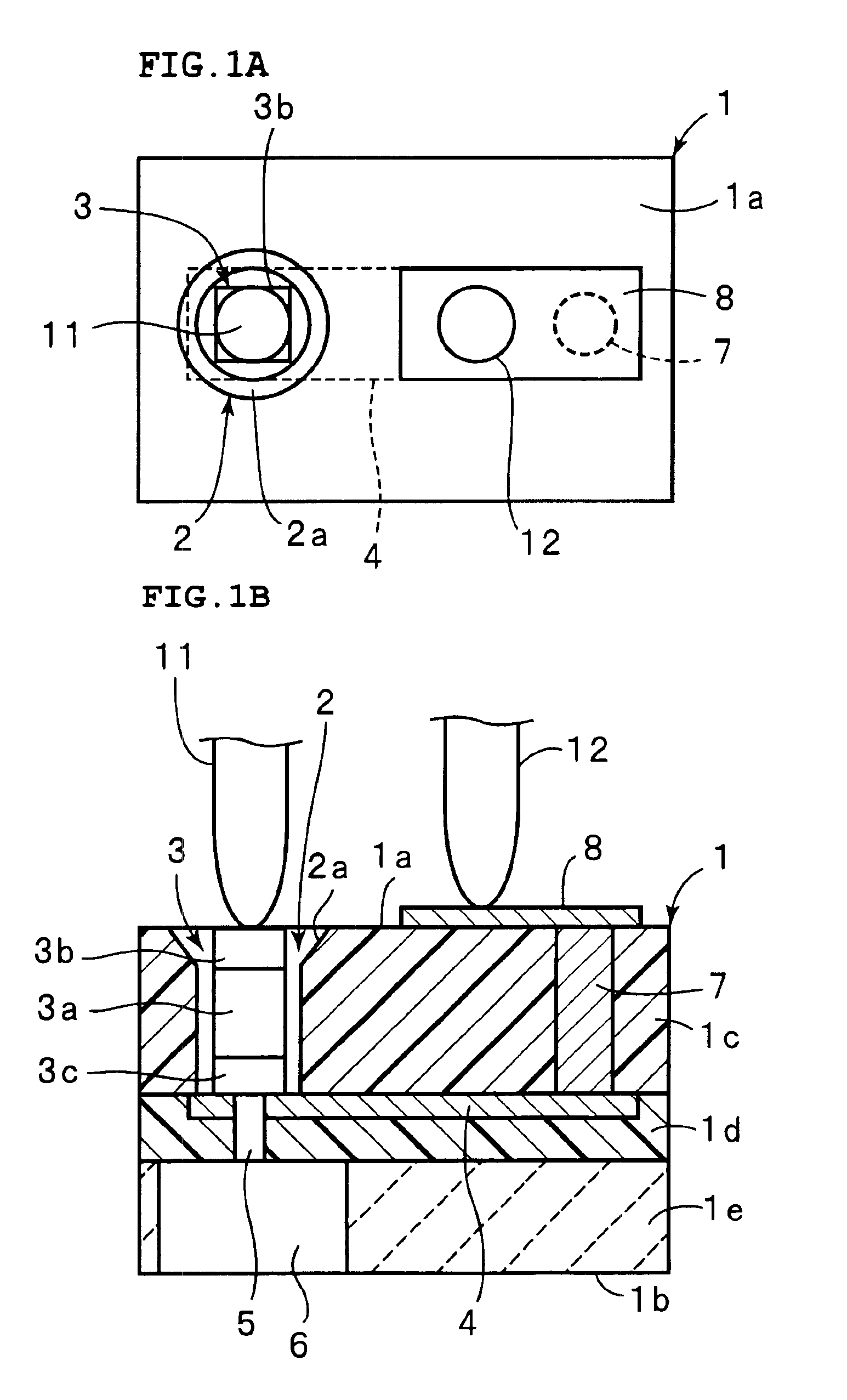
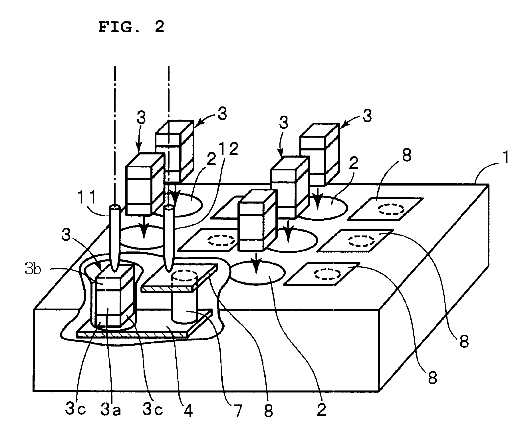
[0029]FIGS. 1A, 1B, and 2 show an apparatus for testing electronic components according to the first preferred embodiment of the present invention.

[0030]Referring to FIGS. 1A and 1B, a unit for testing an electronic component has a cavity 2 on an upper surface 1a of a substrate 1. For accommodating an electronic component 3 (for example, about 0.4 mm in length (L), about 0.2 mm in width (W), and about 0.2 mm in height (H)), the depth of the cavity 2 is the same or greater than the longitudinal length of the electronic component 3, the longitudinal length being vertical in the drawing. That is, the entire electronic component 3 is vertically disposed in the cavity 2. The electronic component 3 may partially project from the substrate 1. In the present preferred embodiment, printed boards 1c, 1d, and an insulating base material 1e are stacked in layers to form the substrate 1. The...


PUM


Abstract

An apparatus for testing an electronic component includes a substrate having a cavity on the upper surface for accommodating an electronic component. The electronic component is inserted into the cavity from a second electrode side. From under the cavity, a connecting conductor extends in a direction that is substantially perpendicular to the thickness direction of the substrate. The connecting conductor is electrically connected to a through-hole electrode. The upper end of the through-hole electrode is further connected to a terminal pad placed on the upper surface of the substrate. Characteristics of the electronic component are measured by attaching a first probe and a second probe to a first substrate of the electronic component and the terminal pad, respectively.

Description

BACKGROUND OF THE INVENTION[0001]1. Field of the Invention[0002]The present invention relates to apparatuses and methods for testing electronic components, for example, for testing characteristics of chip electronic components such as a monolithic ceramic capacitor and a composite high-frequency component. In particular, the present invention relates to an apparatus and a method for testing an electronic component, wherein the electronic component is inserted into a cavity of a substrate and characteristics of the electronic component are measured by a probe.[0003]2. Description of the Related Art[0004]Various types of testing apparatuses are used in the process of measuring and testing characteristics of ceramic electronic components such as a monolithic ceramic capacitor.[0005]FIG. 5 is a perspective view showing an example of known apparatuses for testing electronic components. In this example, characteristics of an electronic component 51 are measured with probes 52 and 53. The ...

Claims


Application Information

Patent Timeline
Patent Type & Authority Patents(United States)
IPC IPC(8): G01R31/01G01R1/04G01R1/02G01R1/06G01R31/00H01G13/00
CPCG01R31/016G01R1/0408
Inventor OKUBO, HIROSHI
Owner MURATA MFG CO LTD
Why Eureka
Try Eureka