
Class D amplifier

a class d amplifier and amplifier technology, applied in the direction of amplifiers with semiconductor devices/discharge tubes, pulse techniques, electronic switching, etc., can solve the problems of unstable operation, increased production costs, and signal not being correctly transmitted from the modulating circuit b>902/b> to the drive controlling circuit b>903

Inactive Publication Date: 2005-08-30
YAMAHA CORP
View PDF1 Cites 11 Cited by
  • Summary
  • Abstract
  • Description
  • Claims
  • Application Information

AI Technical Summary

Benefits of technology

[0017]The invention has been conducted in view of the circumstances noted above. It is an object of the invention to provide a class D amplifier in which output power-MOS transistors can be driven and controlled without using special circuit techniques or electronic components, and the use of a high-breakdown voltage process can be suppressed to a minimum required level.

Problems solved by technology

In this case, the drive controlling circuit 903 must be configured by using high-breakdown voltage transistors, thereby causing the production cost to be increased.
When the power supply system of the drive controlling circuit 903 is configured so as to follow the output signal appearing at the output terminal TO, however, the input threshold of the drive controlling circuit 903 is varied with respect to the level of the pulse signal output from the modulating circuit 902 in the preceding stage, thereby causing a disadvantage that the signal cannot be correctly transmitted from the modulating circuit 902 to the drive controlling circuit 903.
In the first conventional technique, a bootstrap circuit is used in order to convert the level of the signal output from the modulating circuit, and hence there is a problem in that the operation becomes unstable when the signal has a high frequency.
In the second and third conventional techniques, since electronic components such as the insulating transformer and the photocoupler are relatively expensive, the production cost is increased.
Moreover, a space for mounting such electronic components must be assured, and hence the whole amplifier is bulky.
Even when the blocks are formed into separate ICs, therefore, the production cost of each IC is increased.

Method used


Image

  • Class D amplifier
  • Class D amplifier
  • Class D amplifier

Examples


Embodiment Construction

[0041]Hereinafter, an embodiment of the invention will be described with reference to the accompanying drawings.

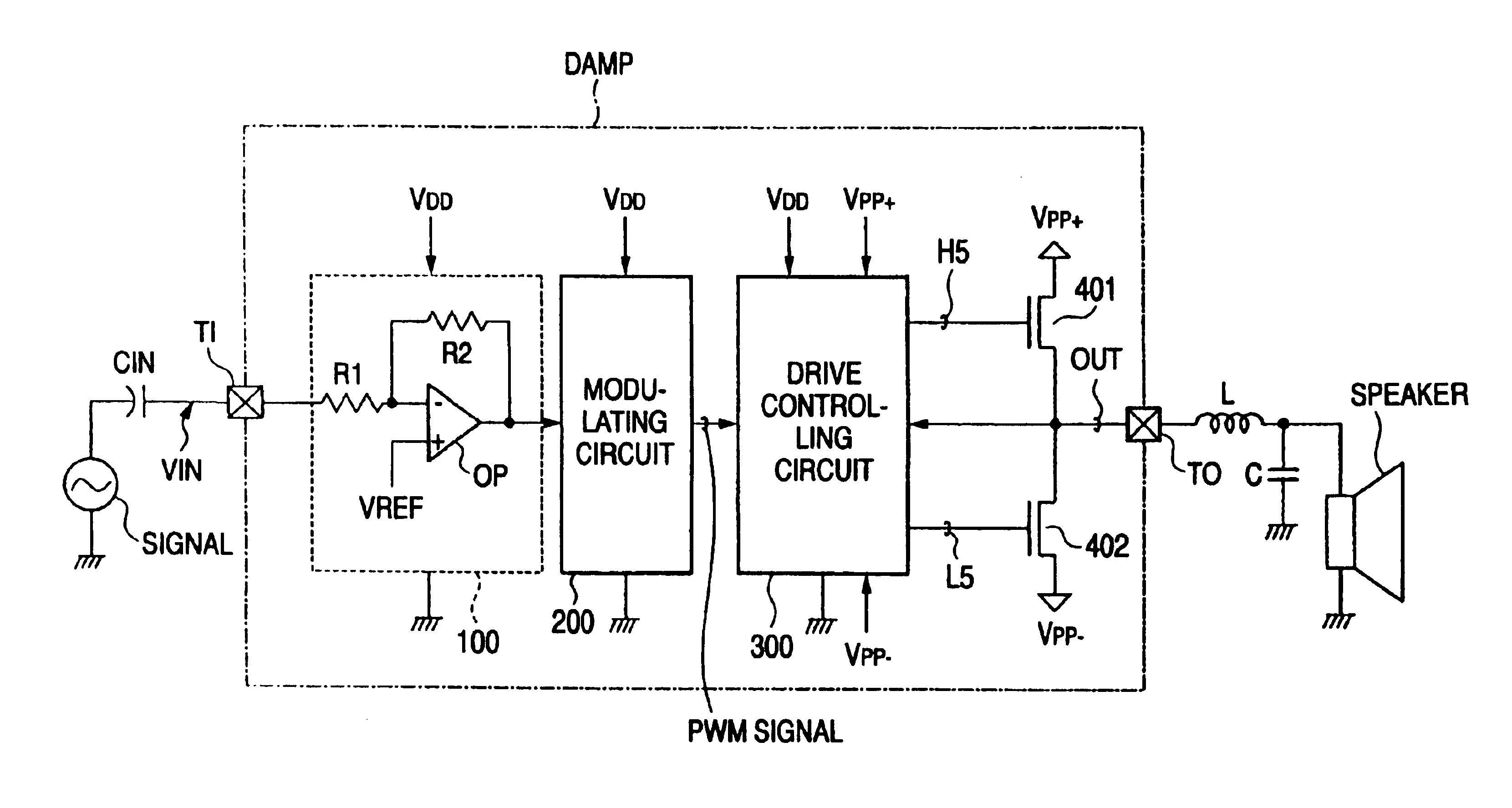
[0042]FIG. 1 shows the configuration of a class D amplifier DAMP according to the embodiment. Referring to the figure, a signal source SIG is a source of a (analog) music signal in which the midpoint of the amplitude is set to the ground potential (0 V). The signal of the signal source SIG is supplied as a music signal VIN to an input terminal TI of the class D amplifier DAMP via an input capacitor CIN. The class D amplifier DAMP is a so-called PWM amplifier, and configured by an input stage 100, a modulating circuit 200, a drive controlling circuit 300, and n-type output power-MOS transistors 401 and 402.

[0043]The input stage 100 is configured by an input resistor R1, a feedback resistor R2(=R1), and an operational amplifier OP. One end of the input resistor RI is connected to the inverting input (−) of the operational amplifier OP, and the other end of the resistor to an...


PUM


Abstract

A complementary signal generating circuit (301) generates first complementary signals (S1, S2) from a PWM signal. A signal converting circuit (302) converts the first complementary signals to second complementary signals (S3, S4 or S5, S6) having a voltage component based on a negative power supply (VPP−). Among the second-complementary signals, the signals (S3, S4) are supplied to a driving circuit (305), and the signals (S5, S6) are supplied to a current driving circuit (303). In response to the signals (S5, S6), the current driving circuit outputs third complementary signals (H3, H4) having a current component that is directed toward the negative power supply (VPP−), to a driving circuit (304). As a result, the driving circuits (304, 305) complementarily drive power-MOS transistors (401, 402).

Description

BACKGROUND OF THE INVENTION[0001]The present invention relates to a class D amplifier (digital amplifier) which converts an analog signal such as a music signal to a pulse signal, and power-amplifies the signal, and more particularly to a circuit technique for driving and controlling output power MOS-transistors.[0002]Conventionally, a class D amplifier is known which receives an analog signal such as a music signal as an input signal, converts the signal to a pulse signal, and then power-amplifies the signal. An output terminal of the amplifier is connected to an input terminal of a loudspeaker via a low-pass filter. In such a class D amplifier, a pulse signal is power-amplified while reflecting the amplitude (information components) of the input signal to the pulse width, and the pulse signal is output. The pulse signal is then passed through the low-pass filter, whereby the power-amplified analog music signal is extracted. The loudspeaker is driven by the music signal. A class D ...

Claims


Application Information

Patent Timeline
Patent Type & Authority Patents(United States)
IPC IPC(8): H03F3/217H03F3/20H03K17/687H03F3/30
CPCH03F3/2171
Inventor TANAKA, YASUOMINORO, MASAO
Owner YAMAHA CORP
Learn More