Magnetic shielding for magnetic random access memory card

Inactive Publication Date: 2005-09-06
SAMSUNG ELECTRONICS CO LTD
View PDF28 Cites 57 Cited by
  • Summary
  • Abstract
  • Description
  • Claims
  • Application Information

AI Technical Summary

Problems solved by technology

One issue encountered by MRAM devices is the presence of stray or external magnetic fields that emanate from sources other than the word and bit lines that are intended to write to a particular memory cell.
Thus, use of MRAM in magnetic field-

Method used


Image

  • Magnetic shielding for magnetic random access memory card
  • Magnetic shielding for magnetic random access memory card
  • Magnetic shielding for magnetic random access memory card

Examples


Embodiment Construction

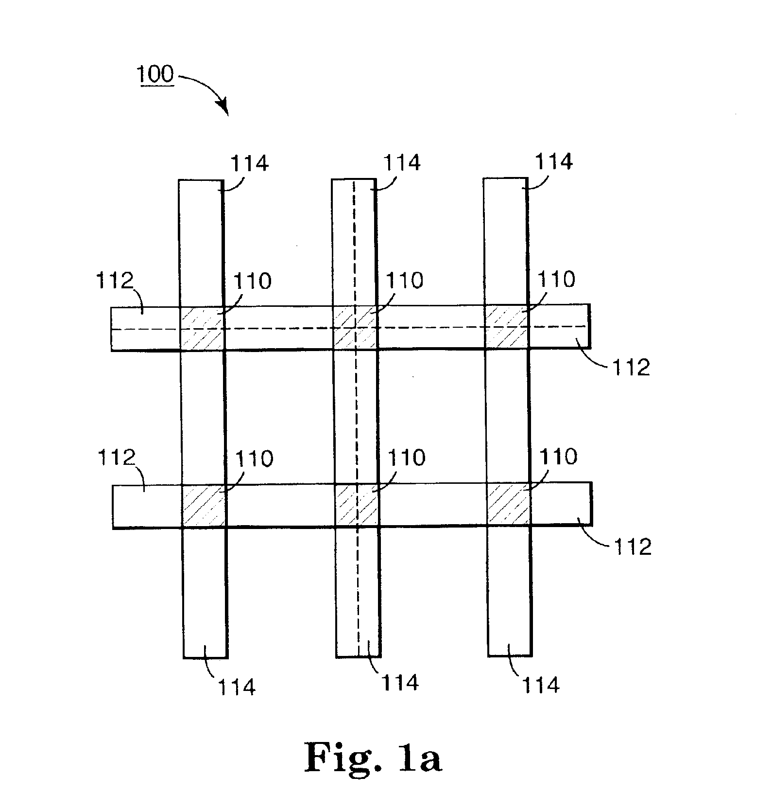
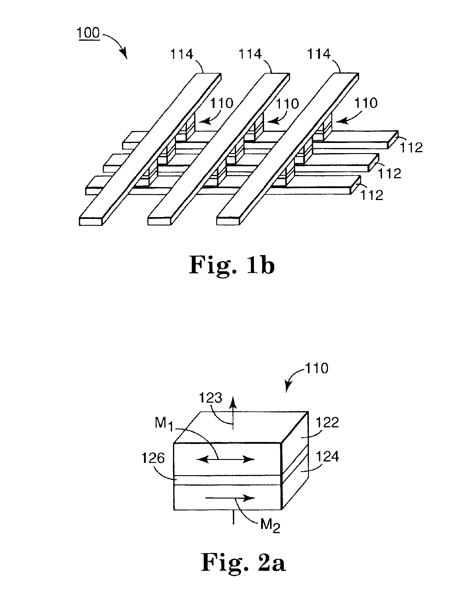
[0021]FIGS. 1a-1b show top plan and perspective views of an embodiment of a simplified MRAM array 100. MRAM array 100 includes memory cells 110, word lines 112, and bit lines 114. Memory cells 110 are positioned at each intersection of a word line 112 with a bit line 114. Word lines 112 and bit lines 114 are write lines arranged in orthogonal relation to one another, and memory cells 110 are positioned between write lines 112, 114, as illustrated in FIG. 1b. For example, bit lines 114 are positioned above memory cells 110 and word lines 112 are positioned below memory cells 110.

[0022]FIGS. 2a-2c illustrate storage of a bit of data in a single memory cell 110. In FIG. 2a, memory cell 110 includes active magnetic data film 122 (the sense layer) and pinned magnetic film 124 (the reference layer), which are separated by dielectric region 126 (the tunnel barrier). The orientation of magnetization in sense layer 122 is not fixed and assumes two stable orientations, as shown by arrow M1. O...


PUM


Abstract

A memory card includes at least one magnetic random access memory supported by a substrate, and a memory card cover disposed over the magnetic random access memory and the substrate to form a memory card, wherein at least one of the substrate and the memory card cover includes magnetic shielding to at least partially shield the magnetic random access memory from external magnetic fields, the memory card cover forming an external portion of the memory card.

Description

BACKGROUND OF THE INVENTION[0001]A magnetic random access memory (MRAM) device includes an array of memory cells. The typical magnetic memory cell includes a layer of magnetic film in which the magnetization is alterable and a layer of magnetic film in which the magnetization is fixed or “pinned” in a particular direction. The magnetic film having alterable magnetization is referred to as a data storage layer or sense layer, and the magnetic film that is pinned is referred to as a reference layer.[0002]Conductive traces (commonly referred to as word lines and bit lines) are routed across the array of memory cells. Word lines extend along rows of memory cells, and bit lines extend along columns of memory cells. Because the word lines and bit lines operate in combination to switch the orientation of magnetization of the selected memory cell (i.e., to write the memory cell), the word lines and bit lines are referred to collectively as write lines. Additionally, the write lines are used...

Claims


Application Information

Patent Timeline
IPC IPC(8): H01L23/552H01L23/48H01L23/498G06K19/00G06K19/07G11C5/00G11C11/15
CPCB82Y10/00G11C7/02G11C7/24G11C11/16H01L23/552H01L23/49816H01L24/48H01L2224/48471H01L2924/01025H01L2924/01057H01L2924/14H01L2924/15311H01L2924/3025H01L2224/16H01L2224/05599H01L2224/16227H01L2224/32225H01L2224/45099H01L2224/48227H01L2224/73265H01L2224/85399H01L2924/00014H01L2924/15192H01L2924/181H01L2924/00012H01L2224/45015H01L2924/207H01L2924/00G11C11/15H05K9/0007
Inventor SPENCER, ANDREW M.LEMUS, CONNIESTOBBS, COLIN
Owner SAMSUNG ELECTRONICS CO LTD
Why Eureka
Try Eureka