Optical resonator waveguide device and method of fabricating the same

a waveguide and optical resonator technology, applied in the direction of optical waveguide light guides, optical elements, instruments, etc., can solve the problems of reducing the operability or usability of the frequency range, affecting the performance of signal light transmission, and restricting the transmittable distance, so as to achieve the effect of expanding the operable or usable frequency rang

Inactive Publication Date: 2005-09-20
NEC CORP
View PDF10 Cites 34 Cited by
  • Summary
  • Abstract
  • Description
  • Claims
  • Application Information

AI Technical Summary

Benefits of technology

[0023]Accordingly, an object of the present invention is to provide an optical waveguide device that makes it possible to expand the operable or usable frequency range toward the higher frequency side, and a method of fabricating the device.

Problems solved by technology

In general, when the transmission rate is raised to 10 Gbit / s or higher, “wavelength dispersion” of an optical fiber will badly affect the performance of signal light transmission conspicuously, which often restricts the transmittable distance by way of optical fibers.
Therefore, after long-distance transmission by way of optical fibers, the arriving time of the components of the signal light will vary according to their wavelength and as a result, the waveform of the modulated signal light will degrade or deform.
Such the waveform degradation or deformation of the modulated signal light makes it difficult to reproduce its original waveform as desired.
However, the compensated optical fiber has many restrictions for use.
Additionally, the compensated optical fiber has a problem that the loss rate of the signal light is relatively high compared with ordinary optical fibers.

Method used


Image

  • Optical resonator waveguide device and method of fabricating the same
  • Optical resonator waveguide device and method of fabricating the same
  • Optical resonator waveguide device and method of fabricating the same

Examples


first embodiment

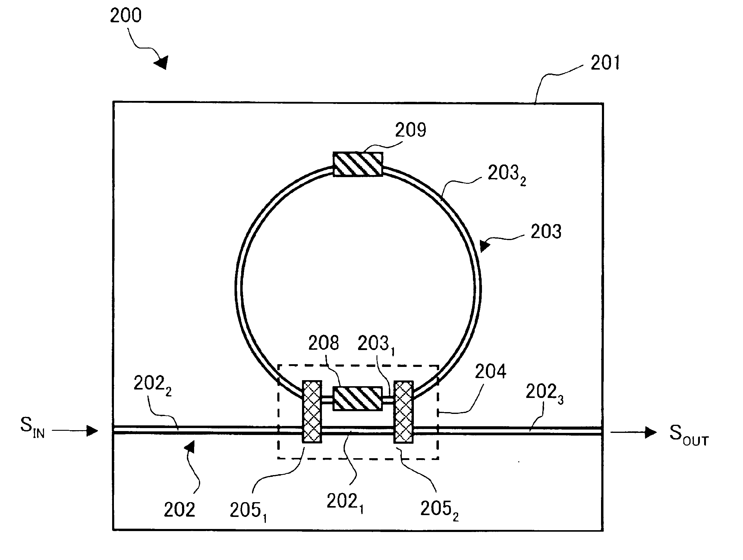
[0152]As shown in FIG. 3, an optical waveguide device 200 according to a first embodiment of the invention comprises an optical waveguide substrate 201, a linear optical input / output waveguide 202, a circular or ring-shaped optical resonator waveguide 203, and a Mach-Zehnder interferometer 204. The linear input / output waveguide 202, the circular resonator waveguide 203, and the interferometer 204 are formed on the substrate 201. The resonator waveguide 203 serves as an optical ring resonator. The interferometer 204 optically interconnects the input / output waveguide 202 and the resonator waveguide 203 with each other. Here, the device 200 is configured as an optical dispersion compensation device.

[0153]The Mach-Zehnder interferometer 204 is formed by first and second multi-mode interference (MMI) optical couplers 2051 and 2052 and first and second optical waveguide arms 2021 and 2031. The first waveguide arm 2021 is a part of the linear waveguide (i.e., the input / output waveguide) 20...

second embodiment

[0192]FIG. 7 shows the structure of an optical waveguide device 300 according to a second embodiment of the invention, in which a suffix “A” is attached to each of the same reference symbols as those used in the first embodiment of FIG. 3. Like the first embodiment, the device 300 is configured as a dispersion compensation device.

[0193]Specifically, the optical waveguide device 300 according to the second embodiment comprises a curved optical waveguide 301 having an intersection or overlap 3016, a Mach-Zehnder interferometer 204A, first and second MMI optical couplers 205A1 and 205A2, a heater 208A for phase adjustment, and a heater 209 for wavelength adjustment. Unlike the device 200 according to the first embodiment of FIG. 3, an input / output optical waveguide and a ring-shaped resonator waveguide are not separated from each other. The input / output optical waveguide and the ring-shaped resonator waveguide are formed by the single optical waveguide 301.

[0194]The waveguide 301, the ...

third embodiment

[0201]FIG. 8 shows the structure of an optical waveguide device 400 according to a third embodiment of the invention, in which a suffix “B” is attached to each of the same reference symbols as those used in the first embodiment of FIG. 3. Like the first embodiment, the device 400 is configured as a dispersion compensation device.

[0202]As shown in FIG. 8, the device 400 according to the third embodiment comprises a curved optical input / output waveguide202B, a ring-shaped optical resonator waveguide 203B serving as an optical ring resonator, a Mach-Zehnder interferometer 204B, a heater 208B for phase adjustment a heater 209B for wavelength adjustment. The waveguides 202B and 203B, the interferometer 204B, the first and second MMI couplers 205A1 and 205A2, and the heaters 208A and 209 are formed on the substrate 201. No intersection exists between the waveguides 202B and 203B, which is unlike the device 300 of the second embodiment of FIG. 7.

[0203]The interferometer 204B has first, sec...


PUM

PropertyMeasurementUnit
total lengthaaaaaaaaaa
lengthaaaaaaaaaa
frequencyaaaaaaaaaa

Abstract

An optical waveguide device expands the operable frequency range toward the higher frequency side. The device includes a single-mode optical resonator waveguide serving as an optical ring resonator, a single-mode optical input/output waveguide located close to the resonator waveguide in an area, and a Mach-Zehnder interferometer formed in such a way as to include a part of the resonator waveguide as its first optical waveguide arm and a part of the input/output waveguide as its second optical waveguide arm in the area. The interferometer has a first optical coupler for optically coupling the first and second waveguide arms with an input-side part of the input/output waveguide and a remaining part of the resonator waveguide due to multiple-mode optical interference, and a second optical coupler for optically coupling the first and second waveguide arms with an output-side part of the input/output waveguide and the remaining part of the resonator waveguide due to multiple-mode optical interference.

Description

BACKGROUND OF THE INVENTION[0001]1. Field of the Invention[0002]The present invention relates to an optical waveguide device and a method of fabricating the same. More particularly, the invention relates to an optical waveguide device using at least one optical ring resonator having an expanded operable or usable frequency range to the upper frequency side, and a method of fabricating the device.[0003]2. Description of the Related Art[0004]In recent years, the transmission rate of optical fiber communication has been increasing continuously. For example, a transmission rate as high as 10 Gigabit per second (Gbit / s) has been actually introduced into commercial optical communication systems. Moreover, in the research and development fields of optical fiber communication, experimental results that 40 Gbit / s, 160 Gbit / s, and higher transmission rates were experimentally realized in optical fiber communication systems have been already reported so far.[0005]In general, when the transmiss...

Claims


Application Information

Patent Timeline
Patent Type & Authority Patents(United States)
IPC IPC(8): G02B6/34H04B10/18G02B6/12G02B6/122G02F1/01
CPCG02B6/29343G02B6/29353G02B6/29394H04B10/25133G02F1/225
Inventor YAMAZAKI, HIROYUKI
Owner NEC CORP
Why Eureka
Try Eureka