Method for fabricating isolation layer in semiconductor device

Inactive Publication Date: 2005-09-27
SK HYNIX INC
View PDF8 Cites 15 Cited by
  • Summary
  • Abstract
  • Description
  • Claims
  • Application Information

AI Technical Summary

Benefits of technology

[0013]Accordingly, the present invention has been made to solve the above-mentioned problems occurring in the prior art, and an object of the present invention is to provide a

Problems solved by technology

Although the isolation insulating layer in the semiconductor device is formed according to a APCVD (Atmosphere Pressure Chemical Vapor Deposition) or a HDPCVD (High Density Plasma Chemical Vapor Deposition) process, limitations exist in their ability to fill fine patterns in a conventional isolation insulating layer as a width of a shallow trench decreases.
A method for depositing fine insulating layer again after depositing the SOD insulating layer in order to solve the above problems has-be

Method used


Image

  • Method for fabricating isolation layer in semiconductor device
  • Method for fabricating isolation layer in semiconductor device
  • Method for fabricating isolation layer in semiconductor device

Examples


Embodiment Construction

[0022]Hereinafter, a preferred embodiment of the present invention will be described with reference to the accompanying drawings. In the following description and drawings, the same reference numerals are used to designate the same or similar components, and so repetition of the description on the same or similar components will be omitted.

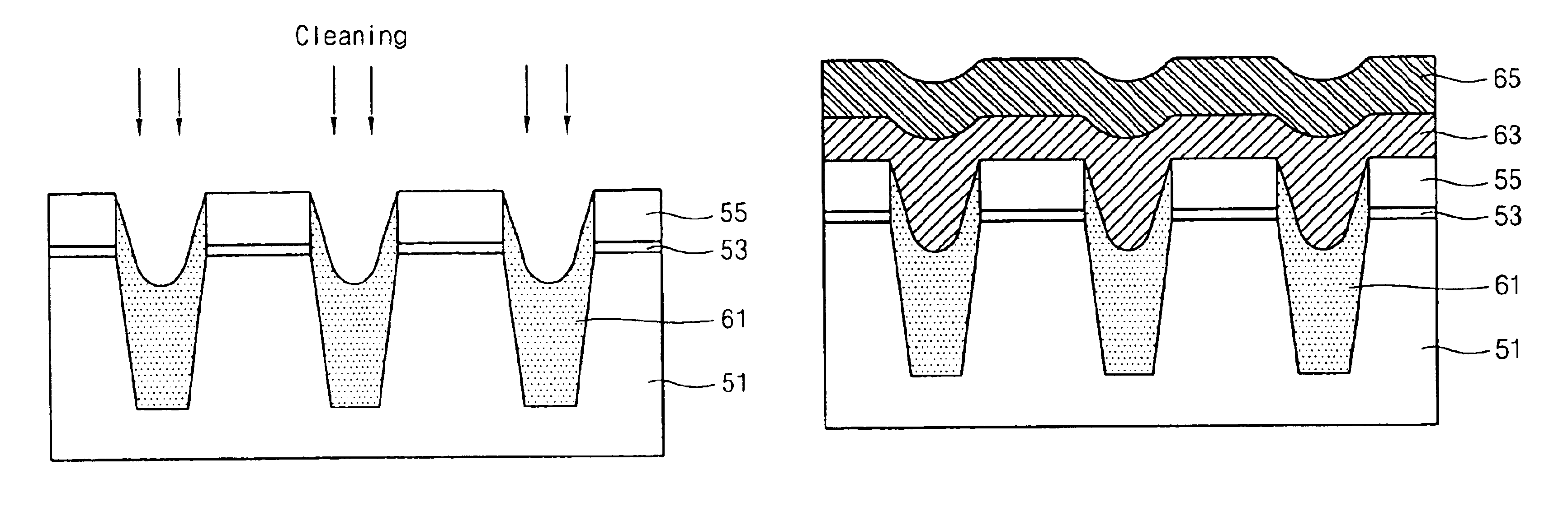
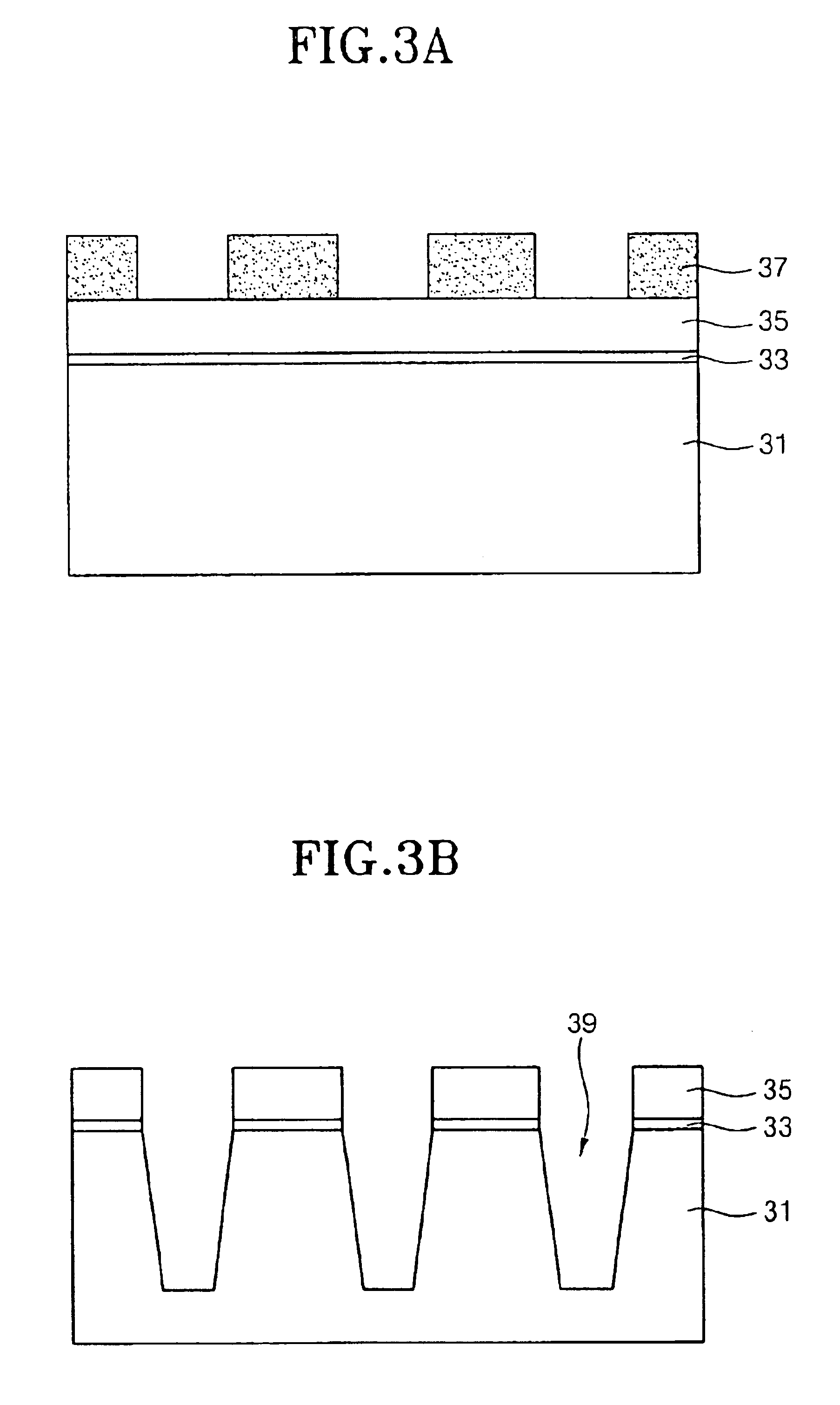
[0023]FIGS. 3A through 3D are cross-sectional views of a process each illustrating a method for fabricating an isolation layer in a semiconductor device according to one embodiment of the present invention, and FIGS. 4A through 4D are cross-sectional views of a process each illustrating a method for fabricating an isolation layer in a semiconductor device according to another embodiment of the present invention.

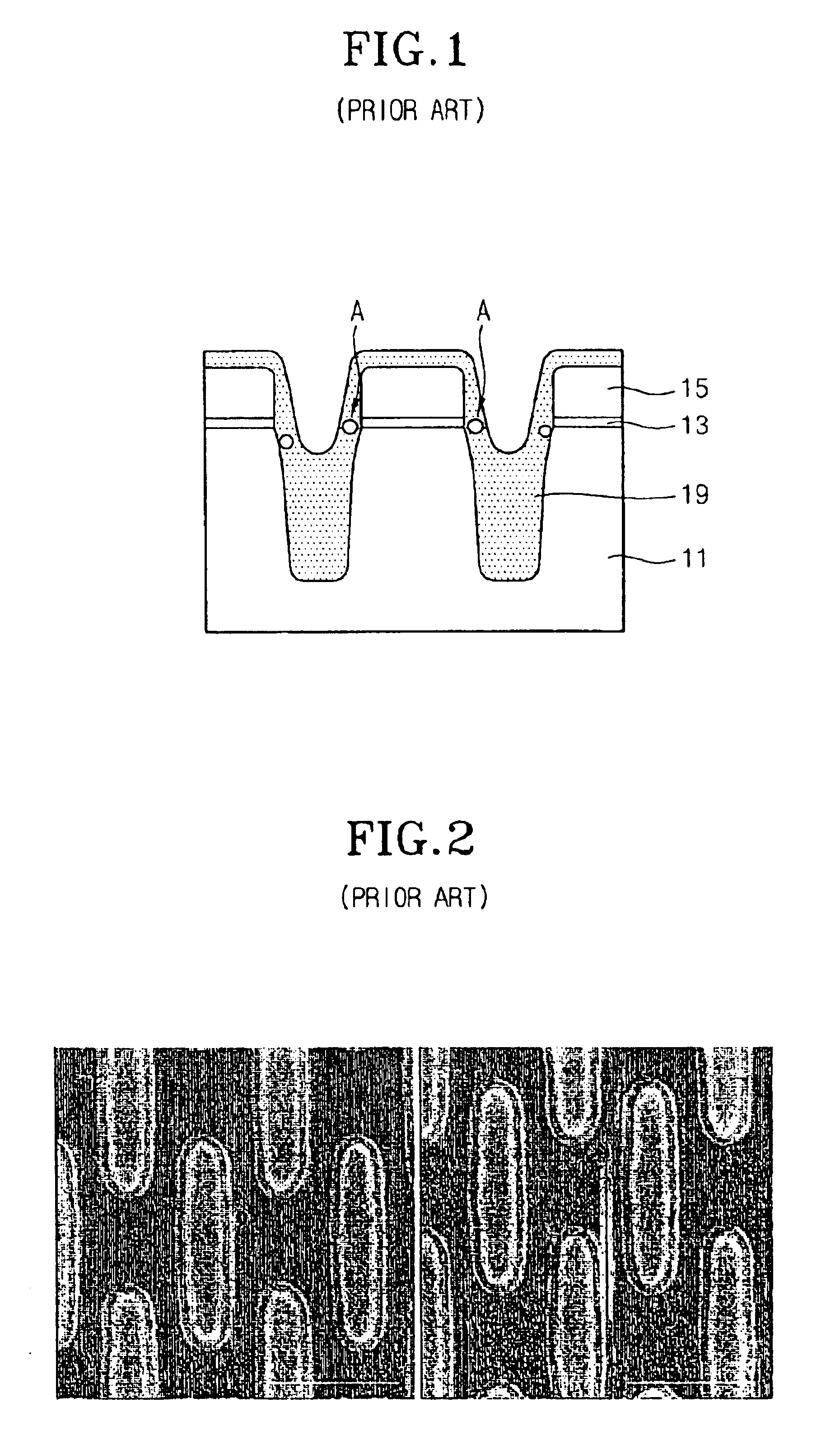
[0024]Further, FIG. 5 is a photograph that shows occurrence of fine pores being decreased in the isolation layer produced by the method for fabricating an isolation layer in a semiconductor device according to the present invention.

[0025]As...


PUM


Abstract

A method for fabricating an isolation layer in a semiconductor device is disclosed. The disclosed method comprises steps of: forming a trench on a semiconductor substrate; forming a flowing insulating layer within the trench; making the insulating layer precise; and forming a precise insulating layer over an upper surface of the whole structure on which the flowing insulating layer is formed. According to the method of fabricating an isolation layer in a semiconductor device, occurrence of fine pores at adjacent active regions of sidewalls in a trench can be prevented.

Description

BACKGROUND OF THE INVENTION[0001]1. Field of the Invention[0002]The present invention relates to a method for fabricating an isolation layer in a semiconductor device, and more particularly to a method for fabricating an isolation layer in a semiconductor device which can improve the ability to fill fine patterns.[0003]2. Description of the Prior Art[0004]As generally known in the art, a width of an isolation insulating layer formed in a STI (Shallow Trench Isolation) process decreases with the advance of integration degree in a semiconductor device. Although the isolation insulating layer in the semiconductor device is formed according to a APCVD (Atmosphere Pressure Chemical Vapor Deposition) or a HDPCVD (High Density Plasma Chemical Vapor Deposition) process, limitations exist in their ability to fill fine patterns in a conventional isolation insulating layer as a width of a shallow trench decreases.[0005]Further, in the case of a flowing SOD (Spin On Dielectric) insulating layer...

Claims


Application Information

Patent Timeline
IPC IPC(8): H01L21/762H01L21/70
CPCH01L21/76224H01L21/762
Inventor AHN, SANG TAECHUNG, SUNG WOONGSOHN, HYUN CHUL
Owner SK HYNIX INC
Why Eureka
Try Eureka