
Ultra low inductance multi layer ceramic capacitor

a ceramic capacitor and low inductance technology, applied in the field of ceramic capacitors, can solve the problems of degrading the effectiveness of the capacitor, affecting the use of high-speed common applications, and parasitic inductance, so as to reduce the physical distance between the external contact terminal and the parasitic inductance. , the effect of low parasitic inductan

Inactive Publication Date: 2005-09-27
MARVELL ASIA PTE LTD
View PDF25 Cites 46 Cited by
  • Summary
  • Abstract
  • Description
  • Claims
  • Application Information

AI Technical Summary

Benefits of technology

The patent text describes a multilayer capacitor with low parasitic inductance. To achieve this, the external contact terminals of the capacitor need to be placed as close as possible to each other to decrease the parasitic capacitance. The patent describes a specific design with first and second electrode plates, a dielectric material, and first and second contacts. The first electrode plate has a contact finger, and the second electrode plate also has a contact finger. The first contact is connected to the contact finger of the first electrode plate, and the second contact is connected to the contact finger of the second electrode plate. The second contact is placed at a predefined minimal distance from the first contact to maintain low parasitic inductance. This design helps to achieve low inductance and minimize interference between the contacts, which improves the performance of the multilayer capacitor.

Problems solved by technology

However, a problem with a conventional capacitor is parasitic inductance.
Parasitic inductance degrades the effectiveness of a capacitor.
Capacitors with large parasitic inductance have low resonance frequency making them unusable for many high-speed common applications.

Method used


Image

  • Ultra low inductance multi layer ceramic capacitor
  • Ultra low inductance multi layer ceramic capacitor
  • Ultra low inductance multi layer ceramic capacitor

Examples


Embodiment Construction

[0028]In the following description of the embodiments, substantially the same parts are denoted by the same reference numerals.

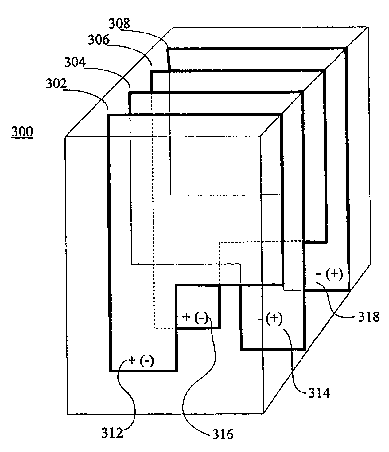
[0029]A multilayer capacitor having a parallelepiped shape with low parasitic inductance is disclosed. In order to maintain a low parasitic inductance in a multilayer ceramic capacitor, the external contact terminals of the capacitor, in one embodiment, need to be placed as close as possible before the occurrence of electrical crosstalk between the external contact terminals and to decrease the parasitic inductance. In other words, a reduction of the physical distance between the external contact terminals of a capacitor causes to decrease the parasitic inductance.

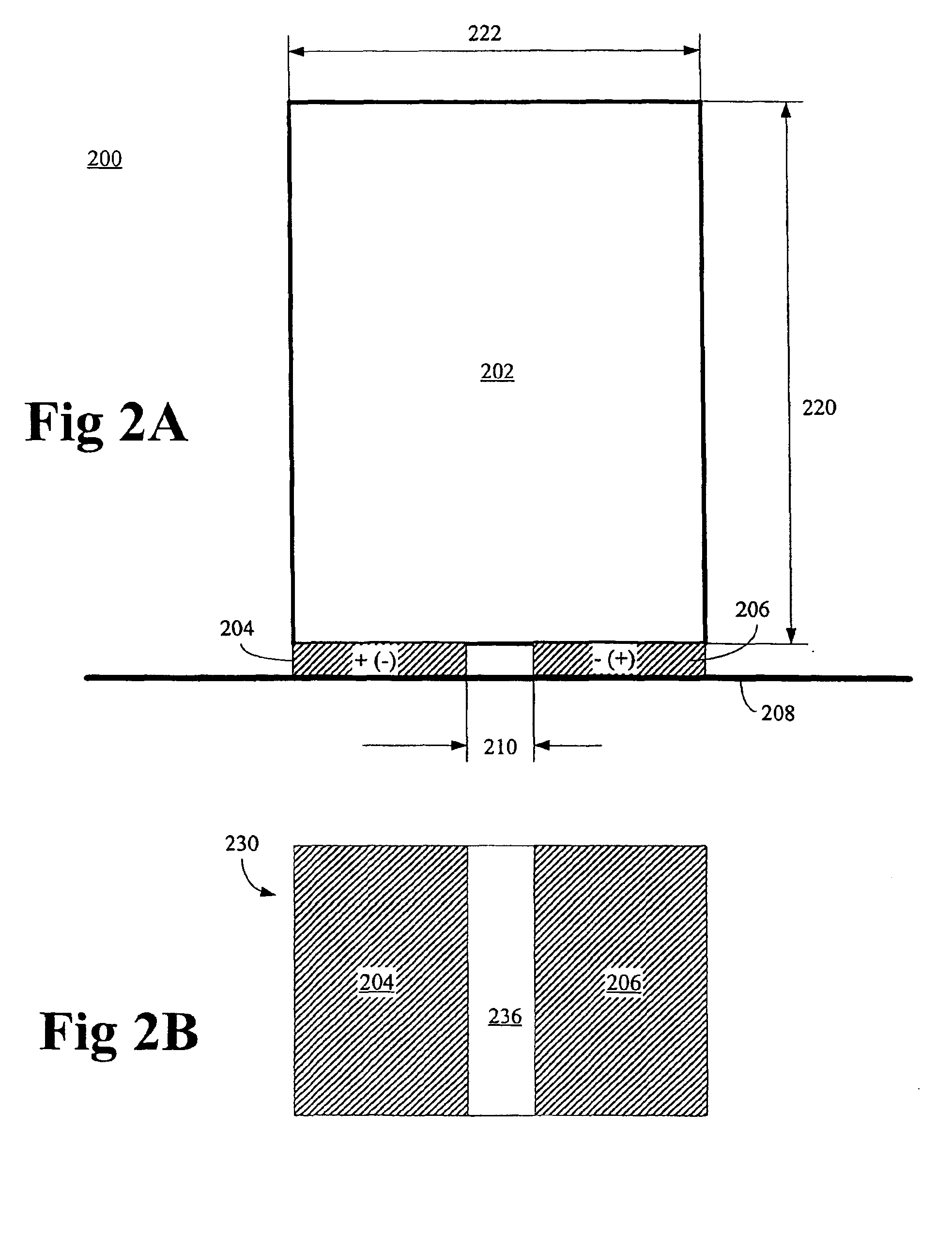
[0030]FIG. 2A is a block diagram 200 illustrating a multilayer capacitor 202, which is mounted on a printed circuit board 208. In one embodiment, capacitor 202 includes two external contacts or contact terminals 204 and 206. Contact bar or terminal 204 is used as a terminal of one polarity while co...


PUM

PropertyMeasurementUnit
distanceaaaaaaaaaa
distanceaaaaaaaaaa
resonance frequenciesaaaaaaaaaa

Abstract

A multilayer capacitor having a low parasitic inductance includes a first electrode, a second electrode, a dielectric, a first contact, and a second contact. The first electrode is substantially rectangular and it includes a first contact finger. The dielectric has a first surface and a second surface, wherein the first and second surfaces are situated opposite with each other. The first surface of the dielectric is coupled with the first electrode. The second electrode is substantially rectangular and it includes a first contact finger. The second electrode is coupled to the second surface of the dielectric. The first contact is coupled to the first contact finger of the first electrode. The second contact is coupled to the first contact finger of the second electrode. The second contact is situated at a minimal space from the first contact to reduce the parasitic inductance.

Description

CROSS-REFERENCE TO RELATED APPLICATIONS[0001]Pursuant to 35 U.S.C. 119(e) and 37 C.F.R. 1.78, the present application claims priority to the provisional applications entitled “Ultra Low Inductance Multi Layer Ceramic Capacitor Structures,” Application No. 60 / 468,380, filed on May 6, 2003, Application No. 60 / 469,475, filed on May 8, 2003, and Application No. 60 / 468,876, filed on May 6, 2003, all of which are hereby incorporated by reference.FIELD OF THE INVENTION[0002]The present invention relates to the field of electronic devices. More specifically, the present invention relates to ceramic capacitors.BACKGROUND[0003]With the increasing performance of computers and network communications, demand for high speed and high-density integrated circuits is increasing. Such high performance integrated circuits (“ICs”) tend to require more sophisticated noise filtering techniques such as decoupling capacitors to enhance the reliability of the devices. Decoupling capacitors are typically plac...

Claims


Application Information

Patent Timeline
Patent Type & Authority Patents(United States)
IPC IPC(8): H01G4/30H01G4/40H05K1/02H01G4/12H01G4/232H01G4/252H02M3/155
CPCH01G4/232H01G4/30H01G4/35H01G4/40H05K1/0231H05K1/0233H05K2201/10515H05K2201/1053
Inventor SUTARDJA, SEHAT
Owner MARVELL ASIA PTE LTD
Learn More