Device for adjusting circuits before encapsulation

Inactive Publication Date: 2005-10-11
STMICROELECTRONICS SRL
View PDF1 Cites 4 Cited by
  • Summary
  • Abstract
  • Description
  • Claims
  • Application Information

AI Technical Summary

Benefits of technology

[0017]The use of “snapback” MOS transistors makes it possible to achieve a short-circuit and thus a resistance inside an integrated circuit by acting on the pins or terminals of the integrated circuit that can be accessed prior to encapsulation. A component formed in this manner takes up little space on a silicon wafer and is therefore inexpensive. The fact that the gate and the source of the MOS transistor are short-circuited ensures permanent blocking of the MOS transistor and keeps it from affecting operation of the rest of the electronic circuit. After breakdown, the MOS transistor can be considered the equivalent of an open circuit.

Problems solved by technology

Some of these terminals may no longer be accessible once the circuit is encapsulated.

Method used


Image

  • Device for adjusting circuits before encapsulation
  • Device for adjusting circuits before encapsulation
  • Device for adjusting circuits before encapsulation

Examples


Embodiment Construction

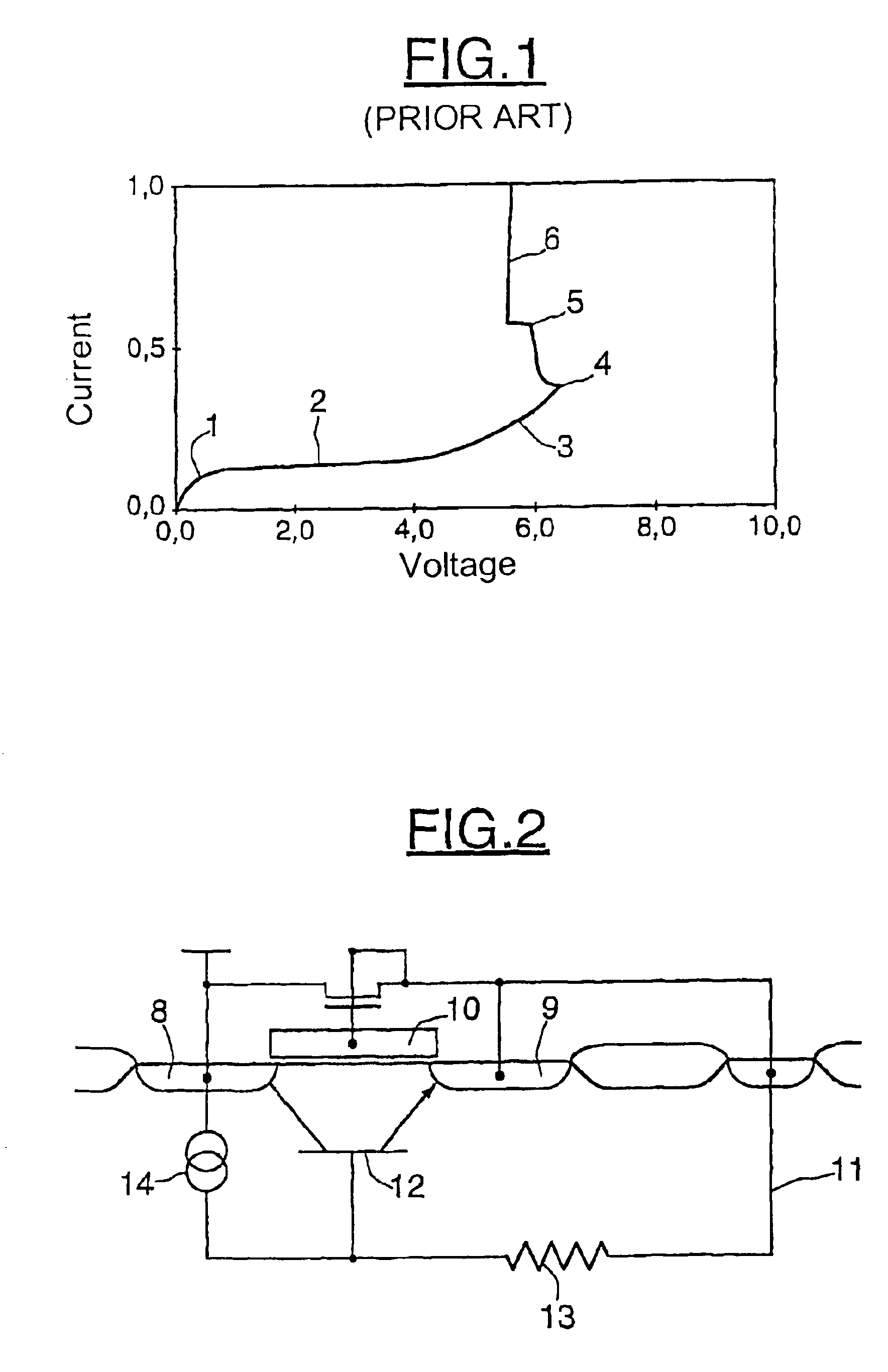
[0025]As can be seen in FIG. 1, where the drain voltage is plotted on the abscissa (horizontal axis) and the drain current is plotted on the ordinate (vertical axis), an n-MOS transistor has four operating regions. Region 1 is the conventional linear operation of a MOS transistor. Region 2 is a saturation-mode operation, in which current varies only very slightly with voltage. Region 3 is known as the avalanche region, with a weakening of the drain / substrate junction caused by avalanche of the junction. Finally, Region 4 is the turn-on of the parasitic bipolar transistor, with the curve showing a first breakdown, referenced 5, which is reversible, and a second breakdown, referenced 6, which is destructive and therefore irreversible.

[0026]Beyond the second breakdown 6, the current varies extremely rapidly with voltage, with the slope of the curve being almost vertical. Since the breakdown process, also known as a second breakdown is irreversible, it is possible to move along the curv...


PUM


Abstract

A device for adjusting an integrated circuit before encapsulation includes a first MOS transistor having a gate and a source connected together, and a body connected to a voltage reference. A first resistor is connected in parallel with the first MOS transistor. A second MOS transistor is connected in series with the first MOS transistor. The second MOS transistor has a gate and a source connected together, and a body connected to the voltage reference. A second resistor is connected in parallel with the second MOS transistor. A first terminal is connected to the source of the first MOS transistor, and a second terminal is connected to the source of the second MOS transistor. The first terminal is accessible externally after the integrated circuit has been encapsulated.

Description

[0001]This application is a national phase of PCT International Application No. PCT / FR02 / 00503 filed on Feb. 11, 2002 under 35 U.S.C. § 371.FIELD OF THE INVENTION[0002]The present invention relates to analog and digital integrated circuits. These circuits desirably use the smallest possible silicon area to reduce costs while still maintaining high precision.BACKGROUND OF THE INVENTION[0003]A silicon wafer that has undergone various steps of etching and / or deposition of conductive, semiconductor or insulation layers is put through a sorting step intended to remove defective circuits. The sorting step is followed by a packaging or encapsulation step.[0004]During the sorting step, each circuit on a wafer is tested to check its conformance,to specifications. A circuit can be considered satisfactory, rejected, or alternatively, a candidate for adjustment. Adjustment is performed by imposing given electrical voltages and / or currents on terminals of the integrated circuit. Some of these te...

Claims


Application Information

Patent Timeline
IPC IPC(8): H01L27/08H01L27/085H01L27/06H01L27/088
CPCH01L27/0629H01L27/0802H01L27/088
Inventor LAVILLE, SEBASTIENPONTAROLLO, SERGE
Owner STMICROELECTRONICS SRL
Why Eureka
Try Eureka