Dynamic random access memory with smart refresh scheduler

a random access and scheduler technology, applied in the direction of information storage, static storage, digital storage, etc., can solve the problems of conflict between the normal dram access and the internal refresh, and achieve the effect of reducing scheduling penalties, facilitating refresh operations, and simplifying circuit implementation

Active Publication Date: 2005-10-11
GLOBALFOUNDRIES U S INC
View PDF12 Cites 18 Cited by
  • Summary
  • Abstract
  • Description
  • Claims
  • Application Information

AI Technical Summary

Benefits of technology

[0004]An object of this invention is to provide a refresh scheduler book unit to manage the internal refresh operation of a DRAM memory without creating a conflict between the internal refresh function and the normal access function.
[0005]It is another object of this invention to provide an efficient refresh schedule algorithm that arbitrates the conflict between normal operation and internal refresh operation. It is also another object to implement the scheduling scheme for managing refresh operation by using the search algorithm that simplifies the circuit implementation and minimizes a penalty from scheduling.
[0006]This invention provides a smart refresh scheduler book unit that can handle or coordinate internal refresh operation and normal access operation. By doing so, the greater frequency of refresh operations caused by a leaky logic cell transistor can be hidden or invisible to the system. It greatly improves memory availability while using a very leaky cell device. The scheduler keeps the refresh status of each memory bank or array by using up / down shift registers and decides which bank to be refreshed. The search operation of this invention is fast and easy to implement.
[0007]The refresh bank search algorithm in this invention is feasible to implement and enables simple circuit implementation while minimizing the penalty caused by a refresh bank search operation.

Problems solved by technology

However, there is conflict between the normal DRAM access and the internal refresh.

Method used


Image

  • Dynamic random access memory with smart refresh scheduler
  • Dynamic random access memory with smart refresh scheduler
  • Dynamic random access memory with smart refresh scheduler

Examples


Embodiment Construction

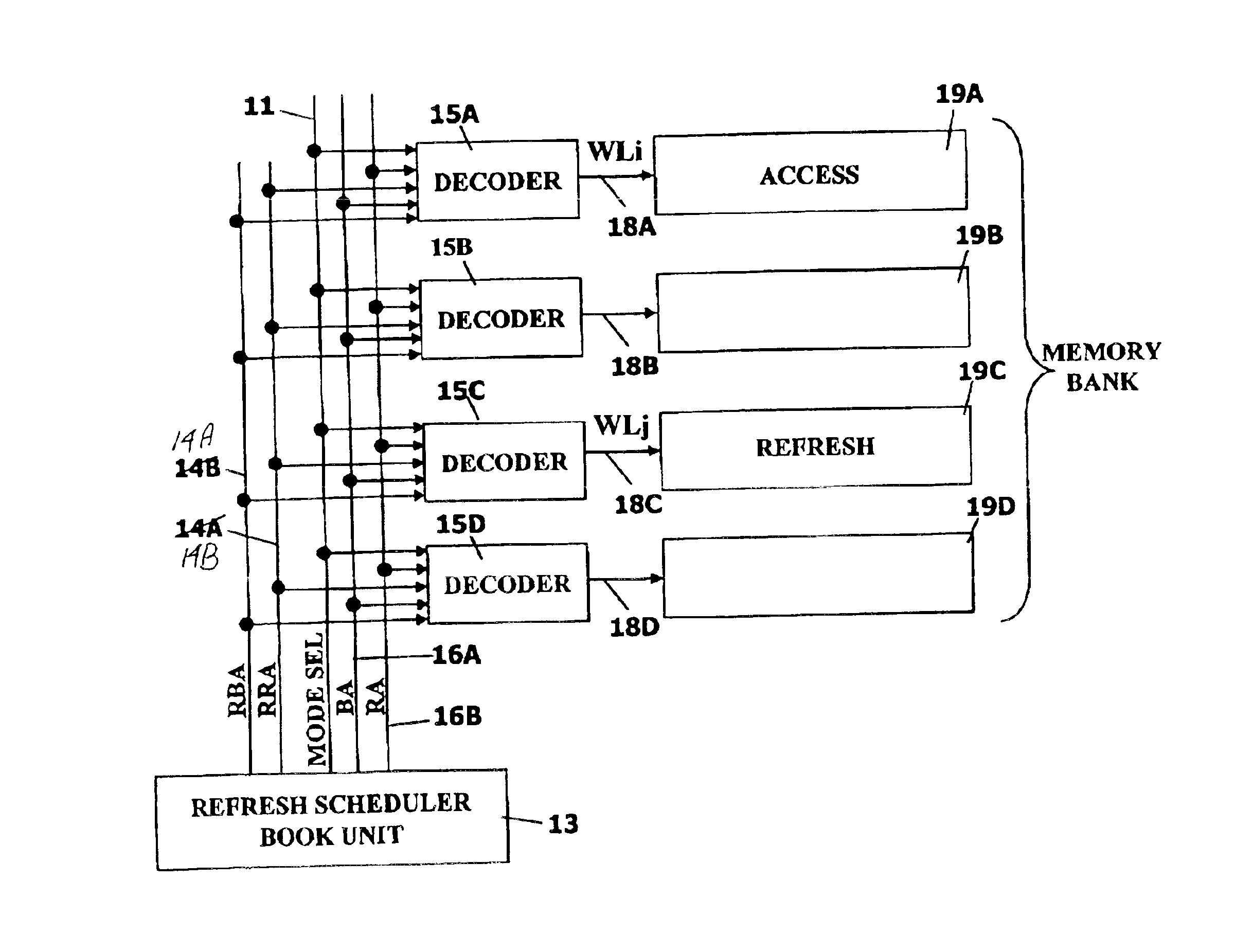
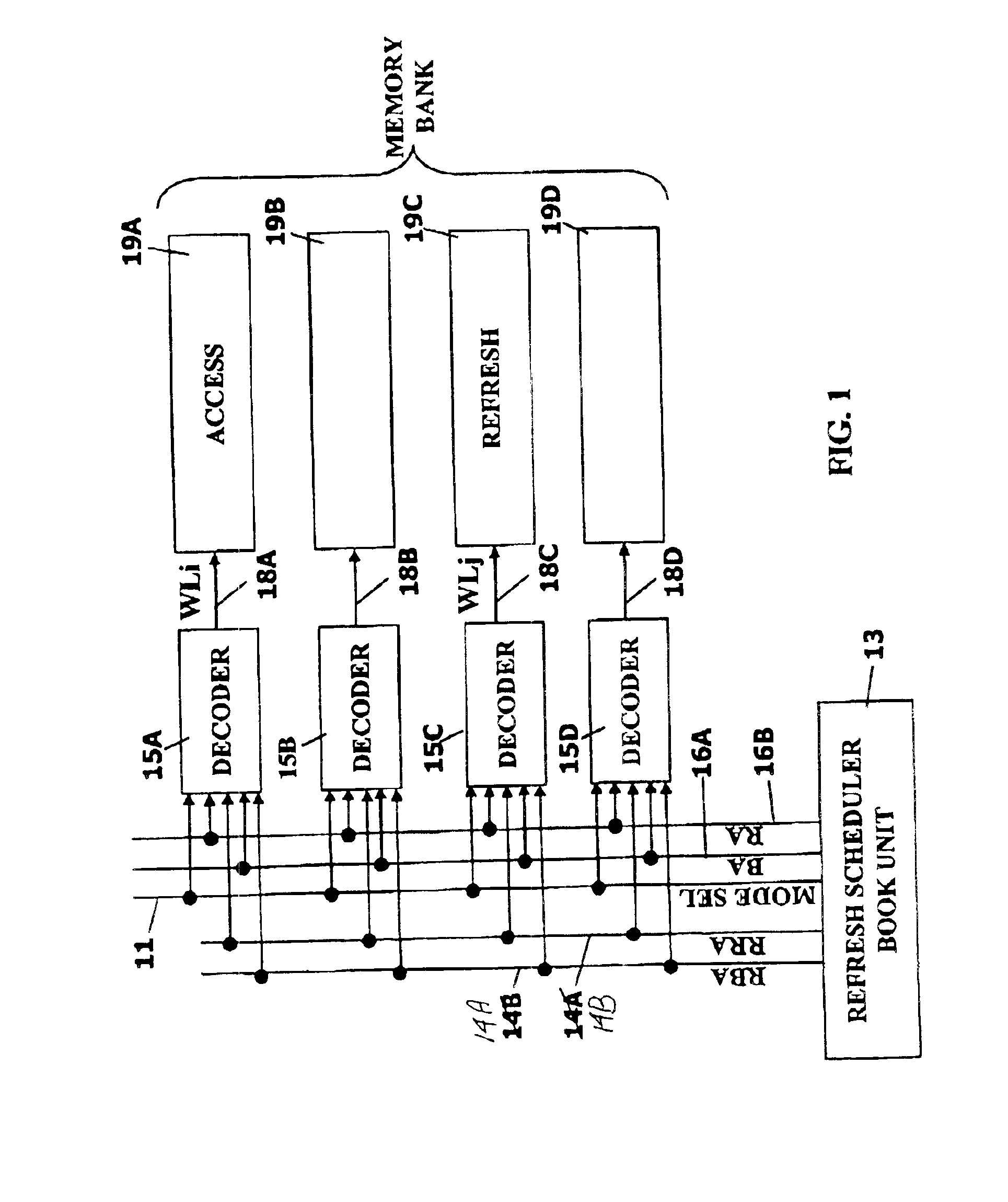
[0022]FIG. 1 shows a multi-bank or multi-array memory with four memory banks 19A-19D to illustrate the basic concept of this invention. In a multi-bank or multi-array memory with several banks 19A-19D in each cycle, only one bank or array is activated for the purpose of normal memory access while one or more of the other banks are activated for the purpose of being refreshed. Therefore, during each cycle, more than one bank or array is activated simultaneously. In FIG. 1 where two banks 19A / 19C are activated at the same time, the first, ACCESS bank 19A is accessed for a normal read or a normal write operation, while a second, REFRESH bank 19C is refreshed. The decision as to whether or not a particular bank will be refreshed is done by a refresh scheduler book unit 13. The refresh scheduler book unit 13 manages the refresh schedule of every bank including ACCESS bank 19A, bank 19B, / REFRESH bank 19C and bank 19D or memory array and issues the global address on lines 14A (RBA), 14B (...


PUM


Abstract

In a DRAM, which includes a plurality of memory banks, there is a pair of separate flag bit registers for each bank with the flag bit registers that are shifted up / down respectively. A comparator for each bank provides a comparator output. An arbiter for each bank is connected to receive a flag bit up signal and a flag bit down signal from the flag bit registers for that bank and the comparator output from the comparator for that bank. The arbiters are connected to receive a conflict in signal and to provide a conflict out signal. The pair of flag bit registers represent a refresh status of each bank and designate memory banks or arrays that are ready for a refresh operation.

Description

BACKGROUND OF INVENTION[0001]This invention relates to a Dynamic Random Access Memory (DRAM) devices, more particularly to logic technology based embedded DRAM devices.[0002]As a solution to the problem of the manufacture of a System-on-Chip (SoC) type of device, use of an eDRAM device has numerous advantages over an embedded Static Random Access Memory (eSRAM). One of the biggest advantages of an eDRAM is the reduced area employed, roughly two to three times less than the area required by an eSRAM. However, the advantage of eDRAMs is diluted by the process complexity and the additional cost caused by the unique process of manufacturing DRAM devices. Therefore, both simplification of the manufacturing process and reduction of the cost of the manufacturing process are required concomitantly maintaining reduced area advantages. Use of logic technology based eDRAMs is such an example. Except for the process of capacitor fabrication, the processing is almost the same as for the logic pr...

Claims


Application Information

Patent Timeline
Patent Type & Authority Patents(United States)
IPC IPC(8): G11C11/406
CPCG11C11/406G11C11/40618G11C2207/104
Inventor KIM, HOKIKIRIHATA, TOSHIAKIHANSON, DAVID R.FREDEMAN, GREGORY J.GOLZ, JOHN
Owner GLOBALFOUNDRIES U S INC
Why Eureka
Try Eureka