High-voltage fast-edge negative pulse generator
A generation device and negative pulse technology, applied in the field of high-voltage fast-edge negative pulse generation devices, can solve the problem that the falling edge time of the board-level negative pulse generation device cannot reach the nanosecond level, is not suitable for integration and miniaturization test requirements, cannot be Meet nanosecond measurement requirements and other issues, achieve high practicability and economic benefits, improve effective measurement accuracy, and low cost
- Summary
- Abstract
- Description
- Claims
- Application Information
AI Technical Summary
Problems solved by technology
Method used
Image
Examples
Embodiment 1
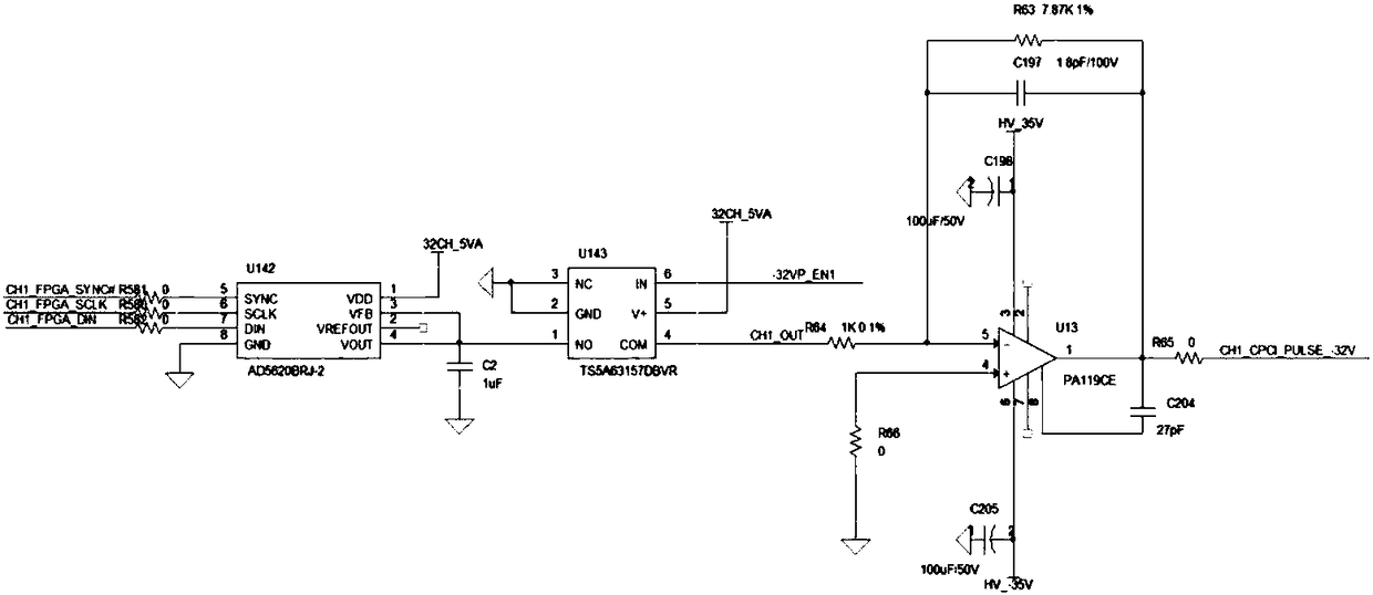
[0020] Such as figure 1 As shown, a high-voltage fast-edge negative pulse generating device is composed of FPGA, D / A conversion device, analog switch and operational amplifier; in this embodiment, the shown FPGA ( figure 1 Not shown in), the D / A converter ( figure 1 Middle U142) is the DAC chip AD5620 of ADI Company, the analog switch ( figure 1 Among U143) is the analog switch TS5A63157 of TI Company, the operational amplifier ( figure 1 Middle U13) selects the operation amplifier PA119CE of APEX Company for use.
[0021] Specifically, the output signal of the FPGA includes a digital voltage signal and a control signal, the digital voltage signal of the FPGA is input into the chip AD5620 through the pin 7 of the chip AD5620, and the control signal of the FPGA is passed through the pin 5 and the pin of the chip AD5620 6 inputs, the control chip AD5620 converts the input digital signal into an analog signal, the analog signal is then output through the pin 4 of the chip AD56...
Embodiment 2
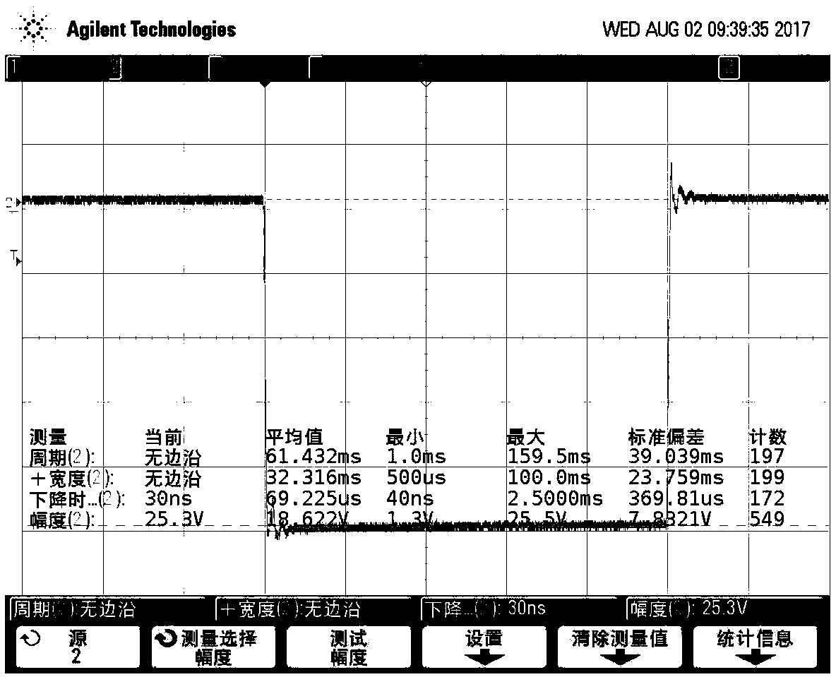
[0024] Based on the high-voltage fast-edge negative pulse generating device described in the above-mentioned embodiments, a simulation test is carried out on it. The resistance R1 is 1kΩ, and the resistance value is 7.87kΩ; by adjusting the capacitance value of the capacitor C1, the test results shown in the following table 1 can be obtained. It can be seen from Table 1 that the value of the capacitor C1 is 1.8pF, which can ensure that the negative pulse generating device The falling edge time is within 30ns, and the waveform amplitude is stable and the ripple is small, such as figure 1 shown.
[0025] Table 1 The falling edge time of the negative pulse generator when the capacitor C1 takes different capacitance values
[0026] serial number
[0027] as table 1 and figure 2 As shown, when the value of the capacitor C1 is 1.8pF, the falling edge time of the negative pulse generator can be within 30ns. And the waveform amplitude is stable and the ripple is small. ...
PUM
| Property | Measurement | Unit |
|---|---|---|
| Resistance | aaaaa | aaaaa |
| Capacitance | aaaaa | aaaaa |
Abstract
Description
Claims
Application Information

