Interleave address generation device and interleave address generation method

a technology of interleave address and generation device, which is applied in the direction of memory address/allocation/relocation, instruments, coding, etc., can solve the problems of considerable processing time and considerable memory space required to generate an interleave address pattern, and achieve the effect of short processing time and small memory spa

Inactive Publication Date: 2005-10-18
PANASONIC CORP
View PDF11 Cites 6 Cited by
  • Summary
  • Abstract
  • Description
  • Claims
  • Application Information

AI Technical Summary

Benefits of technology

[0024]It is an object of the present invention to provide an interleave address generation apparatus and interleave address generation method capable of generating an interleave address pattern with a small memory space and short processing time.

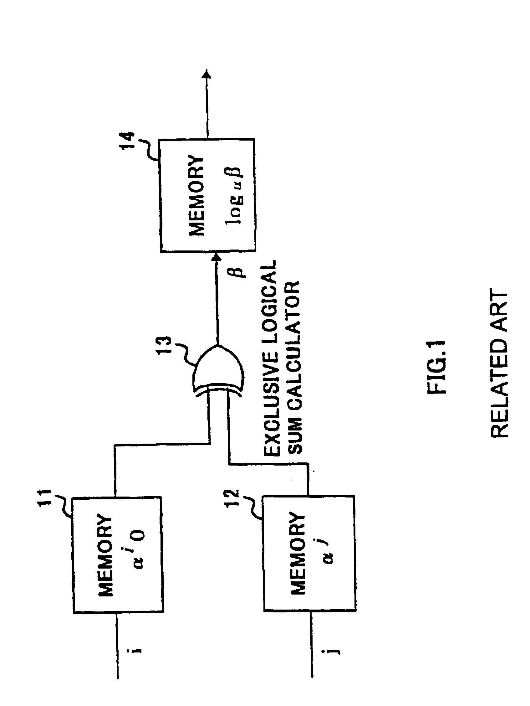
Problems solved by technology

However, the conventional interleave address generation method develops an interleave address pattern created in predetermined units in memory and then performs row rearrangement and an addition of offset addresses, and thus the conventional interleave address generation method has a problem that a considerable memory space and considerable processing time are required to generate an interleave address pattern.

Method used


Image

  • Interleave address generation device and interleave address generation method
  • Interleave address generation device and interleave address generation method
  • Interleave address generation device and interleave address generation method

Examples


embodiment 1

(Embodiment 1)

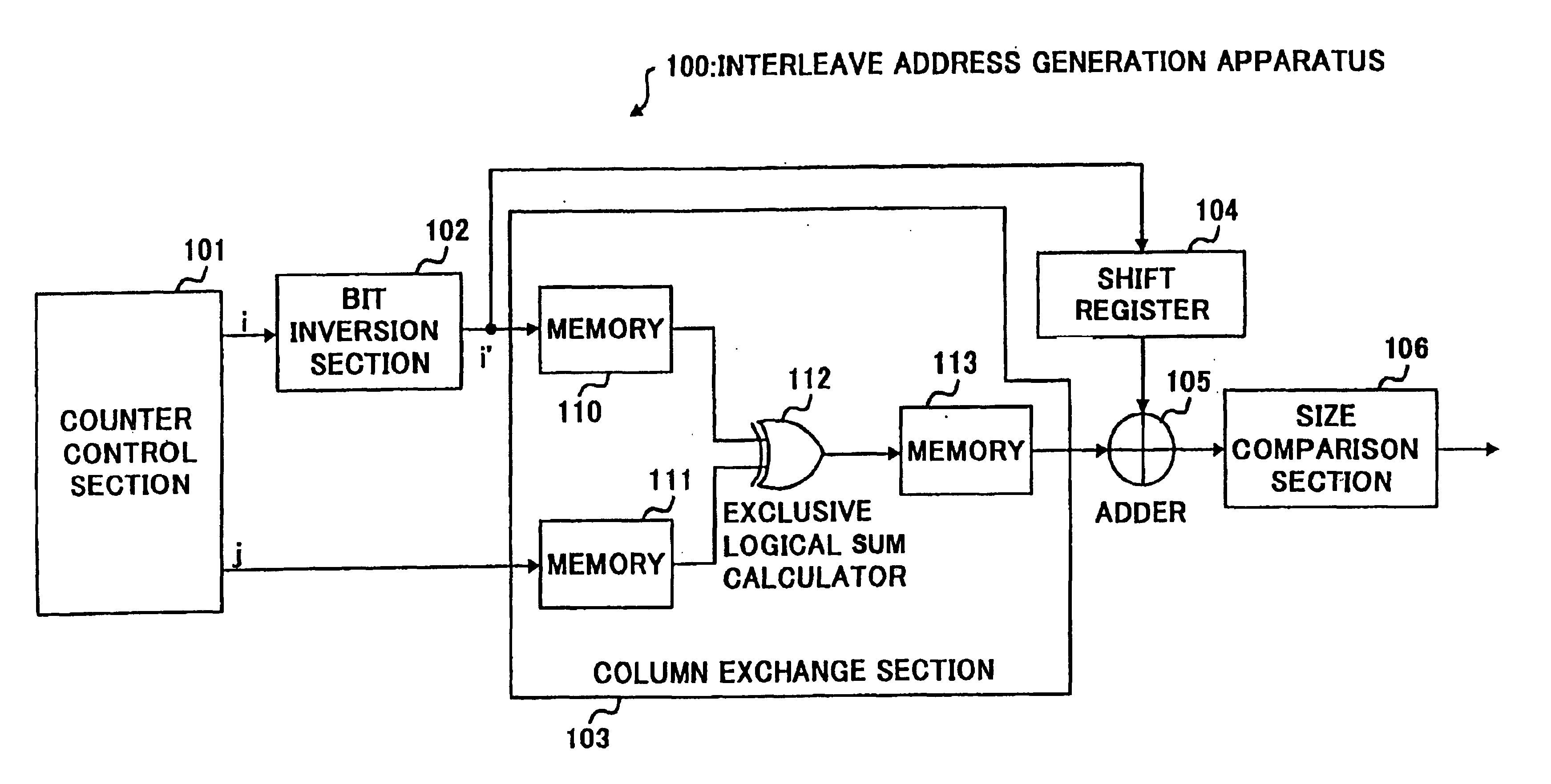
[0049]The interleave address generation apparatus according to Embodiment 1 carries out row rearrangement processing and column rearrangement processing in parallel.

[0050]FIG. 4 is a block diagram showing a configuration of the interleave address generation apparatus according to Embodiment 1 of the present invention.

[0051]Interleave address generation apparatus 100 shown in FIG. 4 is mainly constructed of counter control section 101, bit inversion section 102, column exchange section 103, shift register 104, adder 105 and size comparison section 106.

[0052]Furthermore, column exchange section 103 is mainly constructed of memory 110, memory 111, memory 113 and exclusive logical sum calculator 112.

[0053]In FIG. 4, counter control section 101 outputs row number i (0≦i2) on a two-dimensional array to bit inversion section 102 and column number j (0≦j3) on a two-dimensional array to memory 111.

[0054]For example, when addresses on a 22×23 two-dimensional array are output, co...

embodiment 2

(Embodiment 2)

[0086]FIG. 7 is a block diagram showing a configuration example of an interleave address generation apparatus according to Embodiment 2. However, the configuration common to that in FIG. 4 is assigned the same reference numerals as those in FIG. 4 and detailed explanations thereof are omitted.

[0087]Interleave address generation apparatus 150 in FIG. 7 is different from FIG. 4 in that interleave address generation apparatus 150 is equipped with storage cell array 151 and adds up offset addresses according to the output timing from memory 113.

[0088]In FIG. 7, storage cell array 151 temporarily stores row number i′ output from bit inversion section 102 and then outputs row number i′ to shift register 104.

[0089]For example, storage cell array 151 is constructed of a two-stage storage cell array to adjust the timings of the output from column exchange section 103 and the output from shift register 104 to the timing of the output value i′ from bit inversion section 102.

[0090...

embodiment 3

(Embodiment 3)

[0093]FIG. 8 is a block diagram showing a configuration example of an interleave address generation apparatus according to Embodiment 3.

[0094]In FIG. 8, counter control section 201 outputs row number i of a two-dimensional array to memory 202 and outputs column number j of a two-dimensional array to memory 203.

[0095]Memory 202 stores N(i) corresponding to input i and outputs N(i) corresponding to i output from counter control section 201 to multiplier 204.

[0096]Memory 203 stores M(j) corresponding to input j and outputs M(j) corresponding to j output from counter control section 201 to adder 205.

[0097]Multiplier 204 multiplies N(i) output from memory 202 by the number of columns M and outputs the multiplication result to adder 205.

[0098]Adder 205 adds the multiplication result output from multiplier 204 to M(j) output from memory 203 and outputs the addition result to size comparison section 206.

[0099]When the addition result output from adder 205 is smaller than the s...


PUM


Abstract

Counter control section 101 increments a row number and column number on a two-dimensional array for a block interleave expressed by a matrix two-dimensional array, outputs the incremented numbers as the read address values, bit inversion apparatus 102 performs bit inversion using the read address values as inputs, column conversion section 103 outputs the address values corresponding to the bit inversion output values and the column numbers from counter control section 101 as the column conversion values, shift register 104 bit-shifts the output values of bit inversion apparatus 102 and outputs as the address offset values, adder 106 adds up the address offset values and column conversion values and size comparison section 106 compares the addition value with the interleave size and outputs data which is not greater than the interleave size as address values.

Description

TECHNICAL FIELD[0001]The present invention relates to an interleave address generation apparatus and interleave address generation method, and more particularly, to an interleave address generation apparatus and interleave address generation method ideally applicable to a communication terminal apparatus or base station apparatus.BACKGROUND ART[0002]One of conventional interleave address generation apparatuses and interleave address generation methods is described in the Unexamined Japanese Patent Publication No. HEI 7-212250.[0003]In accordance with the trend of the present times toward the worldwide standardization of a third-generation communication system, standardization plans on interleave are being proposed and GF interleave is one of the interleave methods currently being studied.[0004]This GF interleave is one of block interleaves that perform processing on a two-dimensional array with the number of rows N=2r and the number of columns M=2c. The GF interleave sequentially re...

Claims


Application Information

Patent Timeline
Patent Type & Authority Patents(United States)
IPC IPC(8): H03M13/00H03M13/27
CPCH03M13/2703H03M13/271H03M13/2735H03M13/2771H03M13/00
Inventor IKEDA, TETSUYAYAMANAKA, RYUTARO
Owner PANASONIC CORP
Why Eureka
Try Eureka