
Stacked modular jack

a modular jack and jack technology, applied in the direction of coupling devices, two-part coupling devices, electrical devices, etc., can solve the problems of electronic components that may still suffer from electromagnetic interference which may not be acceptable for high-end signal communication, and the tendency to emit high frequency radiation, so as to achieve the effect of reducing electromagnetic interference and simple structur

Inactive Publication Date: 2005-10-25
HON HAI PRECISION IND CO LTD
View PDF13 Cites 27 Cited by
  • Summary
  • Abstract
  • Description
  • Claims
  • Application Information

AI Technical Summary

Benefits of technology

[0006]It is an object of the present invention to provide a stacked modular jack which has a simple structure and can effectively reduce electromagnetic interference.
[0007]In order to attain the objective above, a stacked modular jack mounted on a mother printed circuit board includes an insulative casing, a magnetic subassembly disposed within the casing and an outer shield enclosing the casing. The magnetic subassembly includes a single molded housing having a receptacle forwardly extending from a main body thereof. A plurality of barriers are formed in a bottom surface of the receptacle for receiving magnetic coils and transformers. The magnetic subassembly further includes an optional magnetic box liner defining a plurality of channels for cooperating with corresponding barriers of the housing for shielding the coils and transformers from other inside components of the modular jack, thereby effectively reducing electromagnetic interference.

Problems solved by technology

A common problem to these high speed modular jacks is their tendency to emit high frequency radiation.
However, the three printed circuit boards are very closed to each other, accordingly electronic components may still suffer from electromagnetic interference which may not be acceptable for high-end signal communication.
Furthermore, the assembly steps become relative complicated.

Method used


Image

  • Stacked modular jack
  • Stacked modular jack
  • Stacked modular jack

Examples


Embodiment Construction

[0019]Reference will now be made in detail to the preferred embodiment of the present invention.

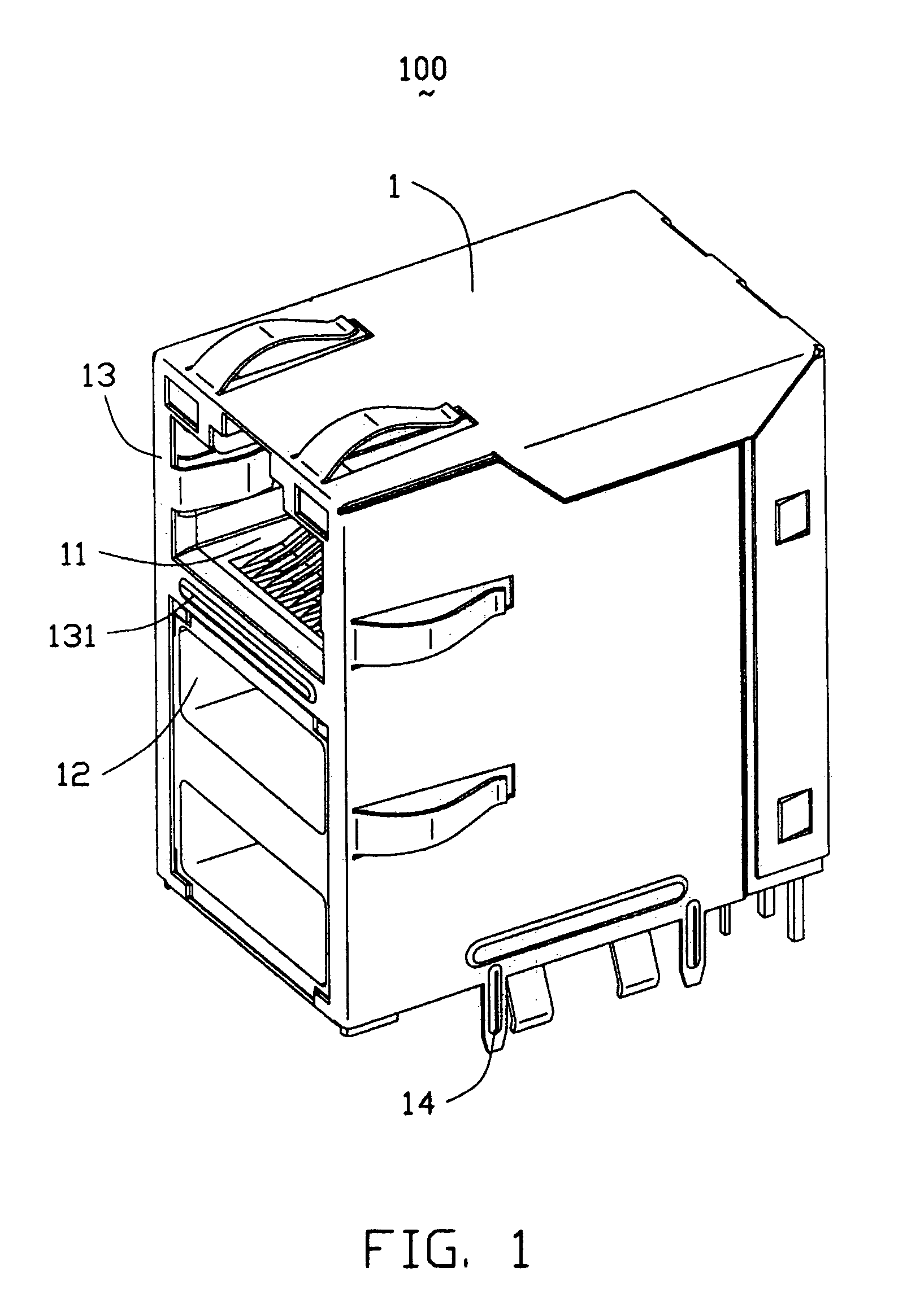
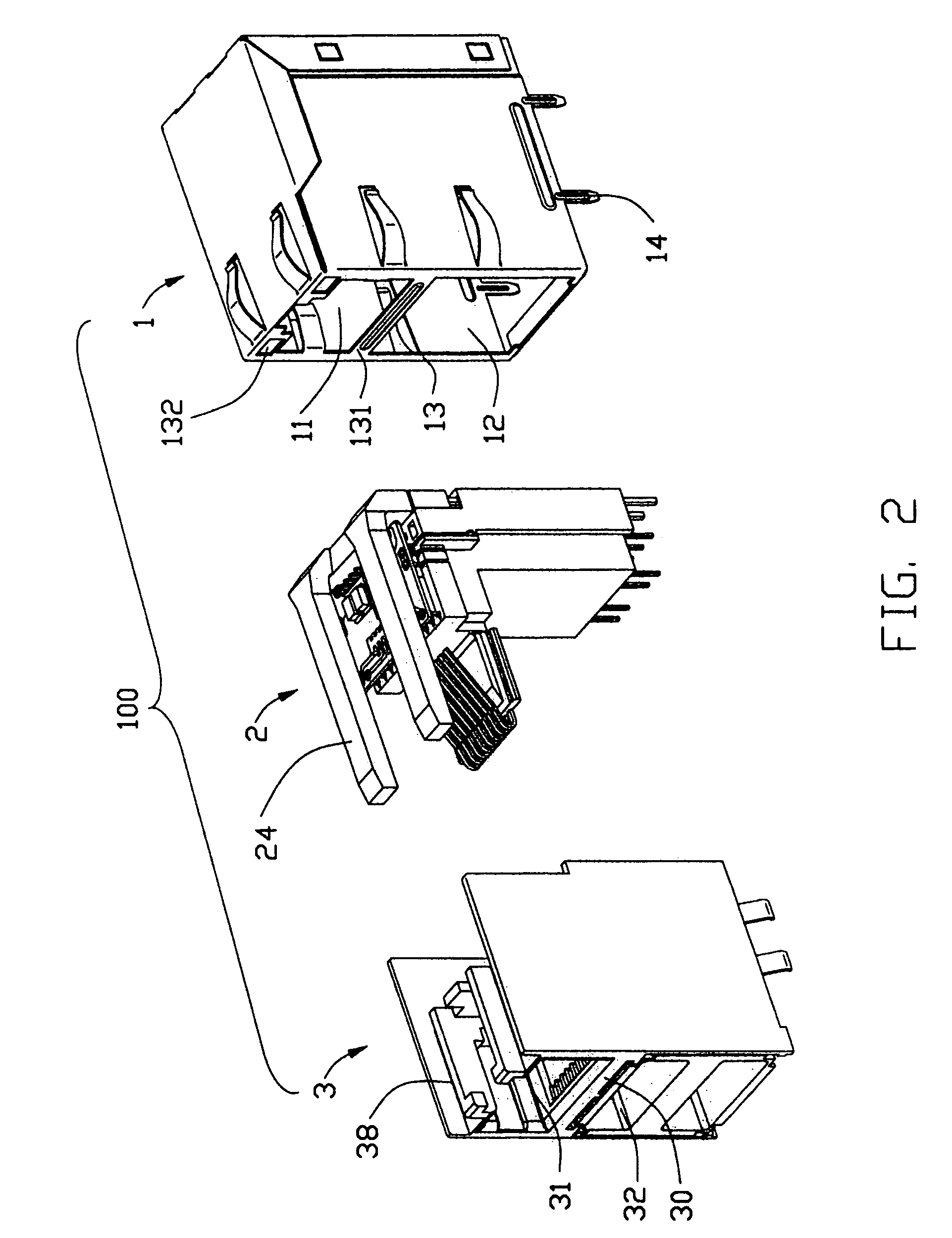
[0020]Stacked modular jack 100 according to the present invention is seen in FIGS. 1–3 and includes an insulative casing 3, an magnetic subassembly 2 disposed within the insulative casing 3 and an outer metal shield 1 optionally enclosing the insulative casing 3 for electromagnetic interference (EMI) protection.

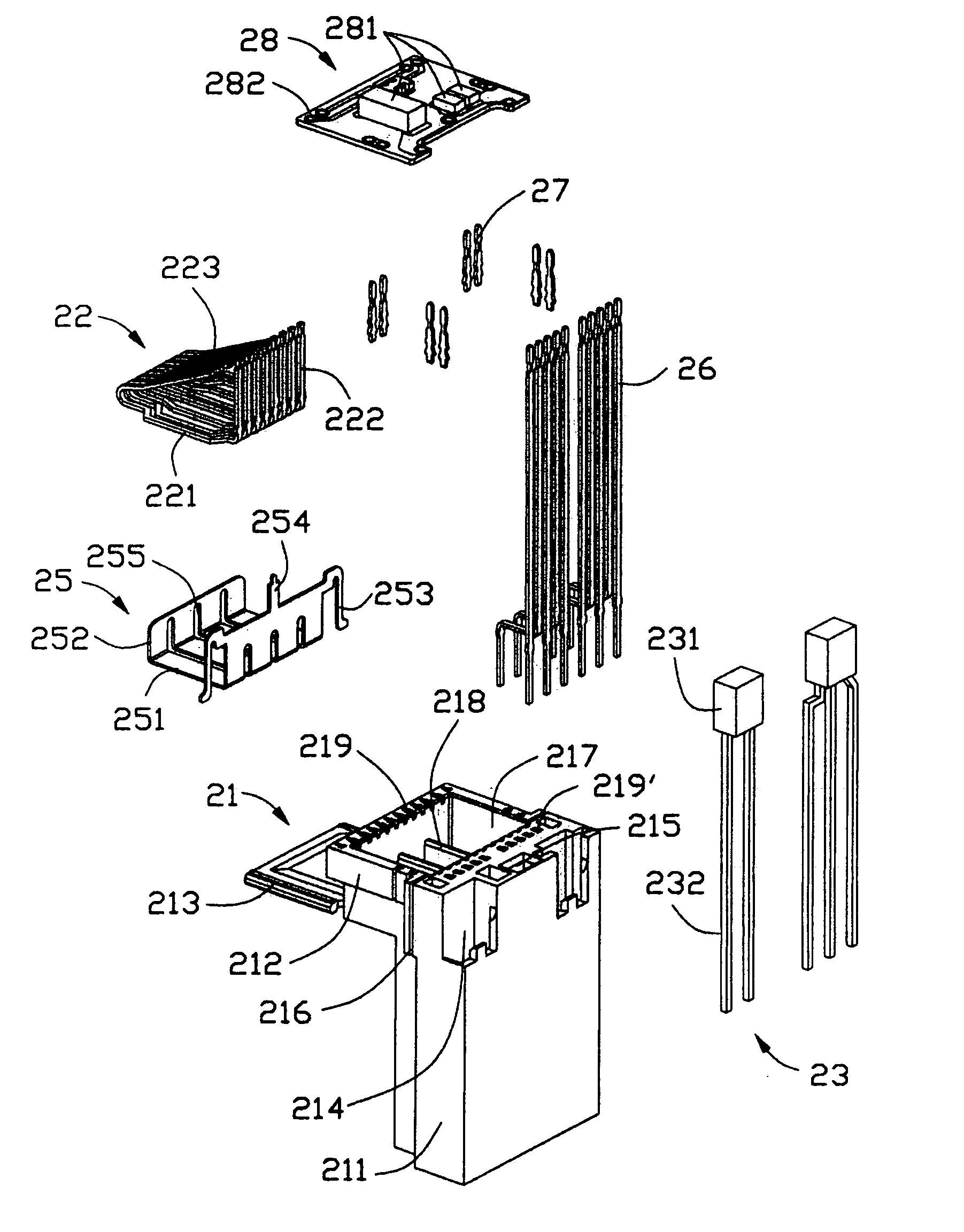
[0021]Referring to FIGS. 5–9, the magnetic subassembly 2 comprises a single molded housing 21, a plurality of contacts 22, a pair of light emitting diodes (LED) 23, a light pipe 24, a magnetic box liner 25 disposed within the housing 21, a first pin array 26 and a second pin array 27 fixed in the housing 21, a daughter printed circuit board 28 disposed above the single molded housing 21 and a plurality of coils 29 retained in the single molded housing 21.

[0022]Referring to FIG. 7, the single molded housing 21 is substantially L-shaped and includes an upright main body 211, a substa...


PUM


Abstract

A stacked modular jack (100) mounted on a mother printed circuit board includes an insulative casing (3), a magnetic subassembly (2) disposed within the casing and an outer shield (1) enclosing the casing. The magnetic subassembly includes a single molded housing (21) having a receptacle (212) forwardly extending from a main body (211) thereof. A plurality of barriers (218) are formed in a bottom surface of the receptacle for retaining magnetic coils and transformers. The magnetic subassembly further includes an optional magnetic box liner (25) defining a plurality of channels (255) for cooperating with corresponding barriers of the housing for shielding the coils and transformers from other inside components of the modular jack, thereby effectively reducing electromagnetic interference.

Description

BACKGROUND OF THE INVENTION[0001]1. Field of the Invention[0002]This invention generally relates to a stacked modular jack and more particularly, to a stacked local area network (LAN) for high speed signal transmission.[0003]2. Description of the Prior Art[0004]It is quite common to use modular jacks for the data transmission in high speed applications such as IEEE 802.3 10 Base-T or 100 Base-T local area networks. A common problem to these high speed modular jacks is their tendency to emit high frequency radiation. There is also a need to provide means for suppressing undesirable noise. As a result, more electrical components are assembled in a modular jack to eliminate electromagnetic interference. U.S. Pat. No. 6,663,437 issued to Korsunsky et al discloses a modular jack including an insulative casing and an electrical subassembly disposed within the housing. The electrical subassembly includes a first and a second contact array assemblies each having a printed circuit board. A f...

Claims


Application Information

Patent Timeline
Patent Type & Authority Patents(United States)
IPC IPC(8): H01R13/66H01R13/719H01R24/00
CPCH01R24/64H01R13/6658H01R13/719
Inventor HYLAND, JAMES H.KORSUNSKY, IOSIF R.WALKER, KEVIN E.
Owner HON HAI PRECISION IND CO LTD
Features
  • Generate Ideas
  • Intellectual Property
  • Life Sciences
  • Materials
  • Tech Scout
  • Unparalleled Data Quality
  • Higher Quality Content
  • 60% Fewer Hallucinations
Learn More