
Electronic device

a technology of electronic devices and circuit boards, applied in the field of electronic devices, can solve the problems of vibration, mechanical strain caused by synchronization with the frequency of ac voltage, and human discomfort in some cases of buzzing noise, so as to suppress the transmission of vibration to circuit boards, suppress the propagation of vibration, and reduce the generation of noise

Active Publication Date: 2005-10-25
TDK CORPARATION
View PDF15 Cites 45 Cited by
  • Summary
  • Abstract
  • Description
  • Claims
  • Application Information

AI Technical Summary

Benefits of technology

[0011]An object of the present invention is to provide an electronic device able to suppress propagation of vibration arising due to piezoelectric and electrostriction phenomena and thereby reduce the generation of noise. Another object of the present invention is to provide a ceramic capacitor or other electronic device able to suppress transmission of vibration to a circuit board etc. by a simple structure.

Problems solved by technology

Such ferroelectric materials, however, have piezoelectric and electrostriction properties, so stress and mechanical strain are caused when the ferroelectric materials are subjected to an electric field.
Further, when an AC voltage is applied to a multilayer ceramic capacitor using such a ferroelectric material, the stress and mechanical strain caused in synchronization with the frequency of the AC voltage is manifested as vibration.
This vibration is transmitted from the terminal electrodes to the board, whereby the board as a whole becomes a sound reflecting surface and a buzzing sound is liable to be generated as noise.
The buzzing noise is unpleasant to humans in some cases.
Further, such buzzing noise has a detrimental effect on the performance and quality of apparatuses having audio circuits or other circuits sensitive to noise.
However, in such multilayer ceramic capacitors, the fact is that the external terminals are high in rigidity and a sufficient effect of preventing vibration has not been obtained.

Method used


Image

  • Electronic device
  • Electronic device
  • Electronic device

Examples


first embodiment

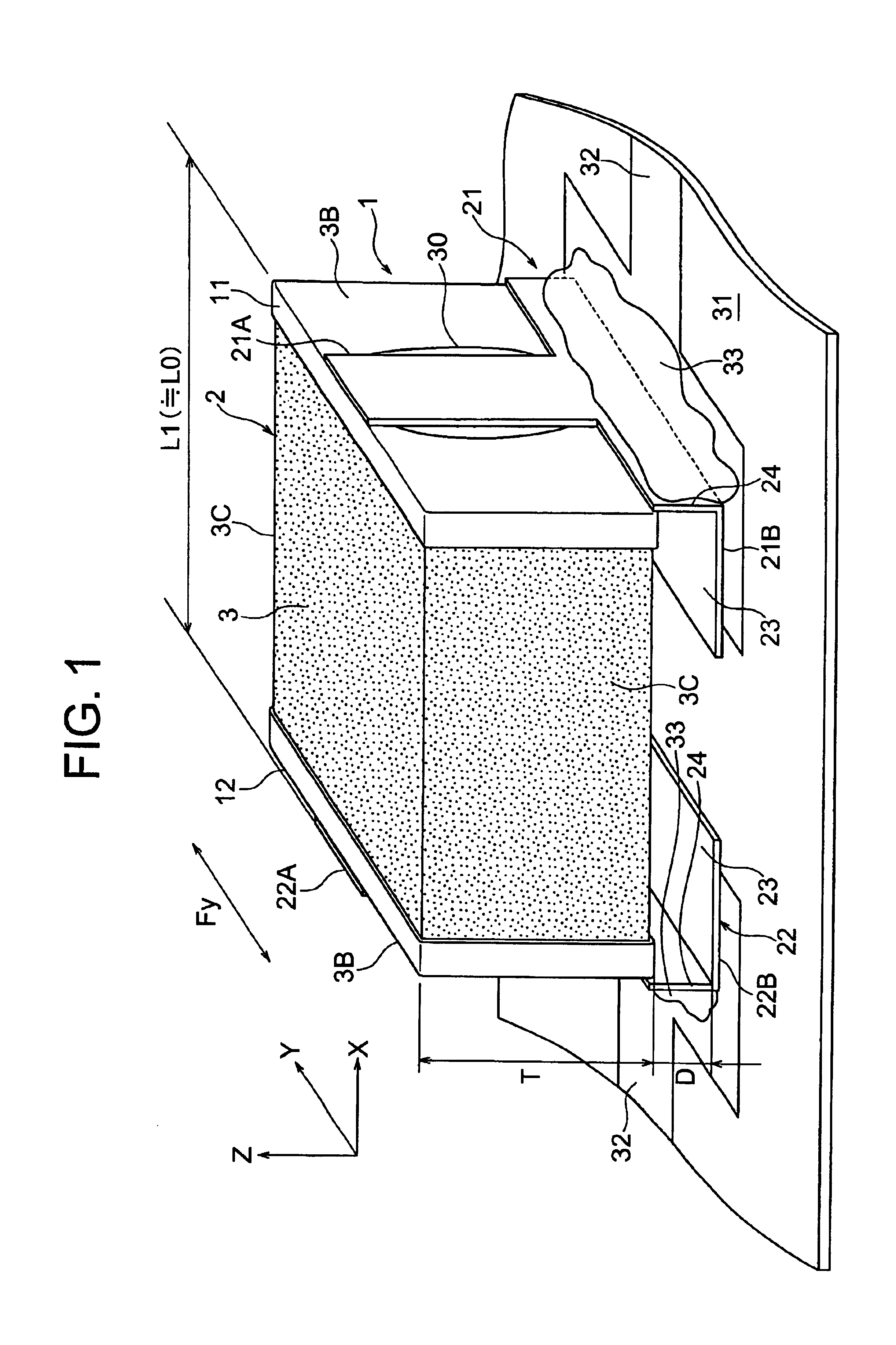
[0082]An electronic device according to a first embodiment of the present invention constituted by a multilayer capacitor 1 is shown in FIG. 1 to FIG. 5. This capacitor 1 has a capacitor body (hereinafter sometimes simply referred to as a “body”). This body 2 has as its main part a dielectric body (main body) 3 comprised of a parallelepiped shaped sintered body obtained by firing a stack of a plurality of ceramic green sheet members.

[0083]As shown in FIG. 5, the dielectric body 3 of the body 2 includes ceramic layers 3A and internal conductor layers 4 and 5. The internal conductor layers 4 and 5 are arranged alternately in the stacking direction (also called “height direction”) Z via the ceramic layers 3A. The number of the internal conductor layers 4 and 5 stacked is not particularly limited, but for example is about 100.

[0084]The centers of these internal conductor layers 4 and internal conductor layers 5 are arranged to be at substantially the same positions as the centers of the...

second embodiment

[0104]Next, an electronic device according to a second embodiment of the present invention constituted by a multilayer capacitor 1a will be shown in FIG. 6 and FIG. 7. Members the same as members explained in the first embodiment are assigned to same notations and overlapping explanations omitted.

[0105]The capacitor 1a of this embodiment has substantially the same structure as the capacitor 1 of the first embodiment. However, as shown in FIG. 6 and FIG. 7, in the present embodiment, the external terminals 21 and 22 have pairs of body supports 25A and 25A. The pairs of body supports are positioned at the two sides of the terminal connection parts 21A and 22A and are formed by bending at substantially right angles to the terminal connection parts 21A and 22A.

[0106]These body supports 25A are bent parallel to the external connection parts 21B and 22B and maintain predetermined distances D from the external connection parts 21B and 22B. These body supports 25A are formed integrally with...

third embodiment

[0111]Next, an electronic device according to a third embodiment of the present invention constituted by a multilayer capacitor will be shown in FIG. 8 and FIG. 9. Members the same as members explained in the first embodiment are assigned to same notations and overlapping explanations omitted.

[0112]This embodiment has substantially the same structure as the first embodiment and exhibits similar actions and effects. However, as shown in FIG. 8 and FIG. 9, in the present embodiment, the external connection parts 21B and 22B are bent into step-like shapes to form the body supports 25B. The widths of the body supports 25B are substantially the same as the widths of the external connection parts 21B and 22B. The bottom surfaces of the terminal electrodes 11 and 12 are placed on the body supports 25B.

[0113]That is, while differing in structure from the second embodiment, since body supports 25B are provided at the external terminals 21 and 22 in the present embodiment as well, in the same...


PUM

PropertyMeasurementUnit
frequencyaaaaaaaaaa
widthaaaaaaaaaa
widthaaaaaaaaaa

Abstract

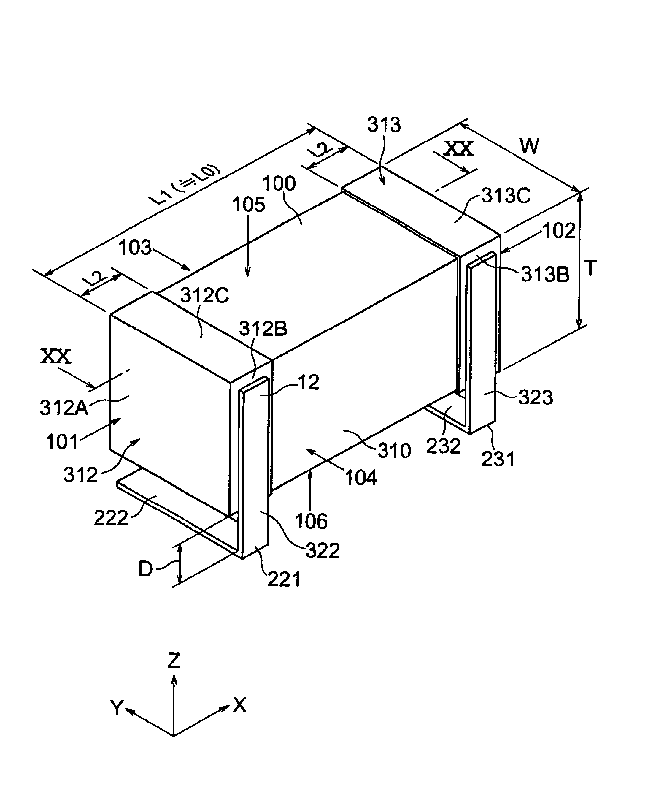
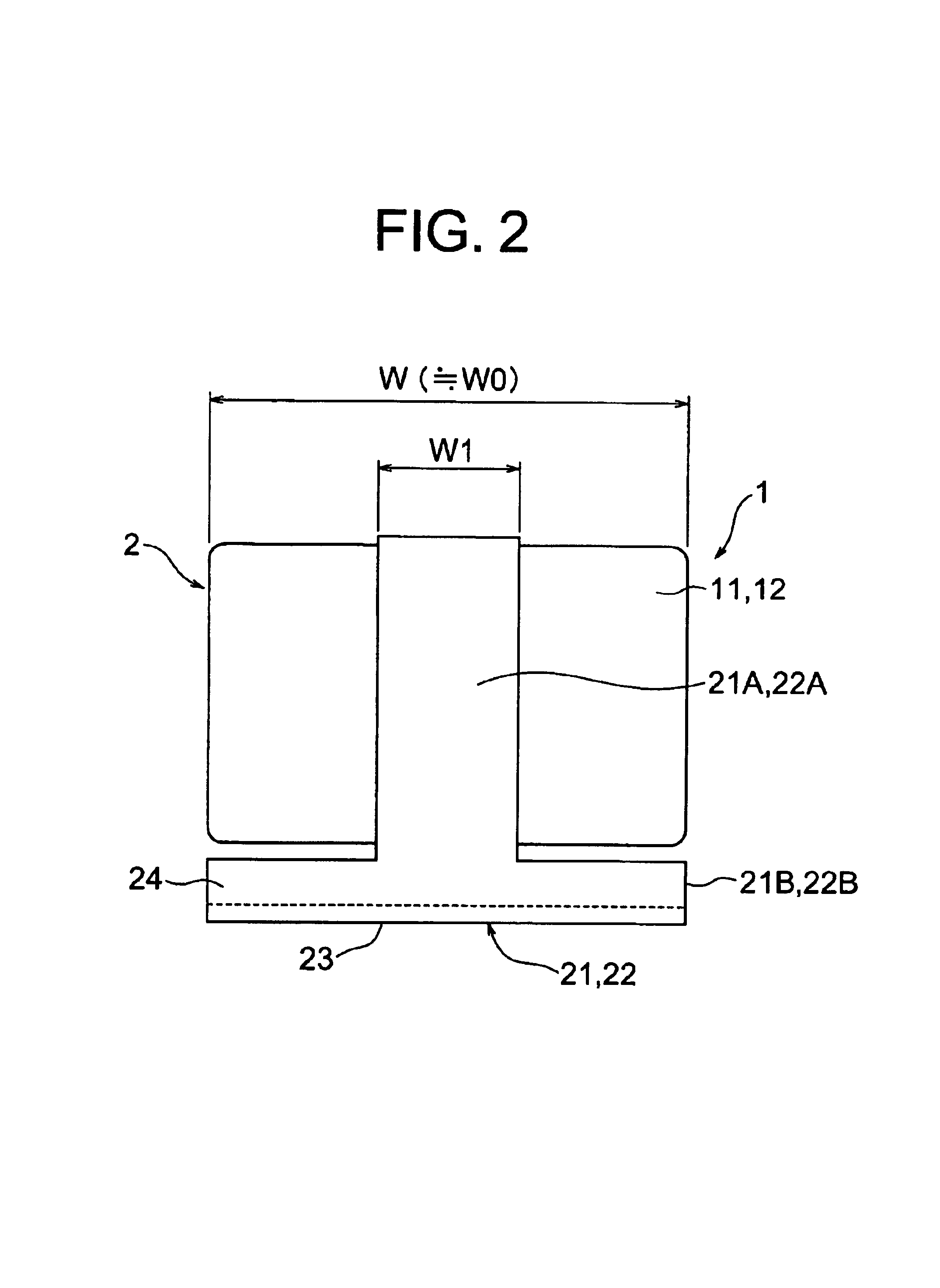
Terminal electrodes 11 and 12 of a main body 2 of a multilayer capacitor 1 are connected to electrode connection parts 21A and 22A of a pair of external terminals 21 and 22 formed by a metal material. At the bottom part of the electrode connection part 21A, an external connection part 21B connected to the electrode connection part 21A is formed. At the bottom part of the electrode connection part 22A, an external connection part 22B connected to the electrode connection part 22A is formed. The widths of the terminal electrodes 11 and 12 and the widths of the external connection parts 21B and 22B are substantially the same, but the widths of the electrode connection parts 21A and 22A are formed narrower. Due to this, propagation of vibration can be suppressed and generation of noise reduced.

Description

BACKGROUND OF THE INVENTION[0001]1. Field of the Invention[0002]The present invention relates to an electronic device able to suppress propagation of vibration caused by piezoelectric and electrostriction phenomena and thereby reduce noise, more particularly relates to a ceramic capacitor used for an audio circuit or other circuit sensitive to noise or used for a smoothing capacitor for a switching power source.[0003]2. Description of the Related Art[0004]There have been remarkable advances in technology for reducing the thickness of layers and technology for increasing the number of layers of multilayer ceramic capacitors in recent years. Capacitors having high electrostatic capacities comparable to those of aluminum electrolytic capacitors have been marketed. As the ceramic materials for forming the stacks of such multilayer ceramic capacitors, barium titanate and other ferroelectric materials having relatively high dielectric constants are generally used.[0005]Such ferroelectric ...

Claims


Application Information

Patent Timeline
Patent Type & Authority Patents(United States)
IPC IPC(8): H05K3/34H01G4/12H01G2/06H01G4/228H02N2/00
CPCH01G2/065H01G4/228H05K3/3426H05K2201/10946H05K2201/10636Y02P70/50H01G4/12
Inventor TOGASHI, MASAAKIAHIKO, TAISUKEYOSHII, AKITOSHITAKEDA, ATSUSHI
Owner TDK CORPARATION
Learn More