Printed board unit for optical transmission and mounting method

a printed board unit and optical transmission technology, applied in the direction of optical elements, instruments, optical waveguide light guides, etc., can solve the problems of dirt and dust, inability to stabilize the performance of individual optical modules, and the gap formed between the light emitting (light receiving) element and the optical waveguide substrate b>1/b>, so as to achieve accurate control and enhance the transmission efficiency of laser beams

Inactive Publication Date: 2005-10-25
FUJITSU LTD
View PDF9 Cites 7 Cited by
  • Summary
  • Abstract
  • Description
  • Claims
  • Application Information

AI Technical Summary

Benefits of technology

[0008]It is an object of the present invention to provide a mounting structure for mounting a surface light emitting (light receiving) element on an optical wave-guide substrate characterized in that: the gap between the light emitting (light receiving) element and the optical wave-guide substrate does not fluctuate, so that the interval can be accurately controlled and the transmitting efficiency of a laser beam can be enhanced; and the gap cannot be clogged with dirt and dust.

Problems solved by technology

Accordingly, the light emitting or light receiving characteristic is changed, so that the performance of the individual optical module can not be stabilized.
Further, there is a problem in which a gap formed between the light emitting (light receiving) element and the optical wave-guide substrate 1 can be clogged with dirt and dust.

Method used


Image

  • Printed board unit for optical transmission and mounting method
  • Printed board unit for optical transmission and mounting method
  • Printed board unit for optical transmission and mounting method

Examples


Embodiment Construction

[0022]By referring to the accompanying drawings, embodiments of the present invention will be explained below.

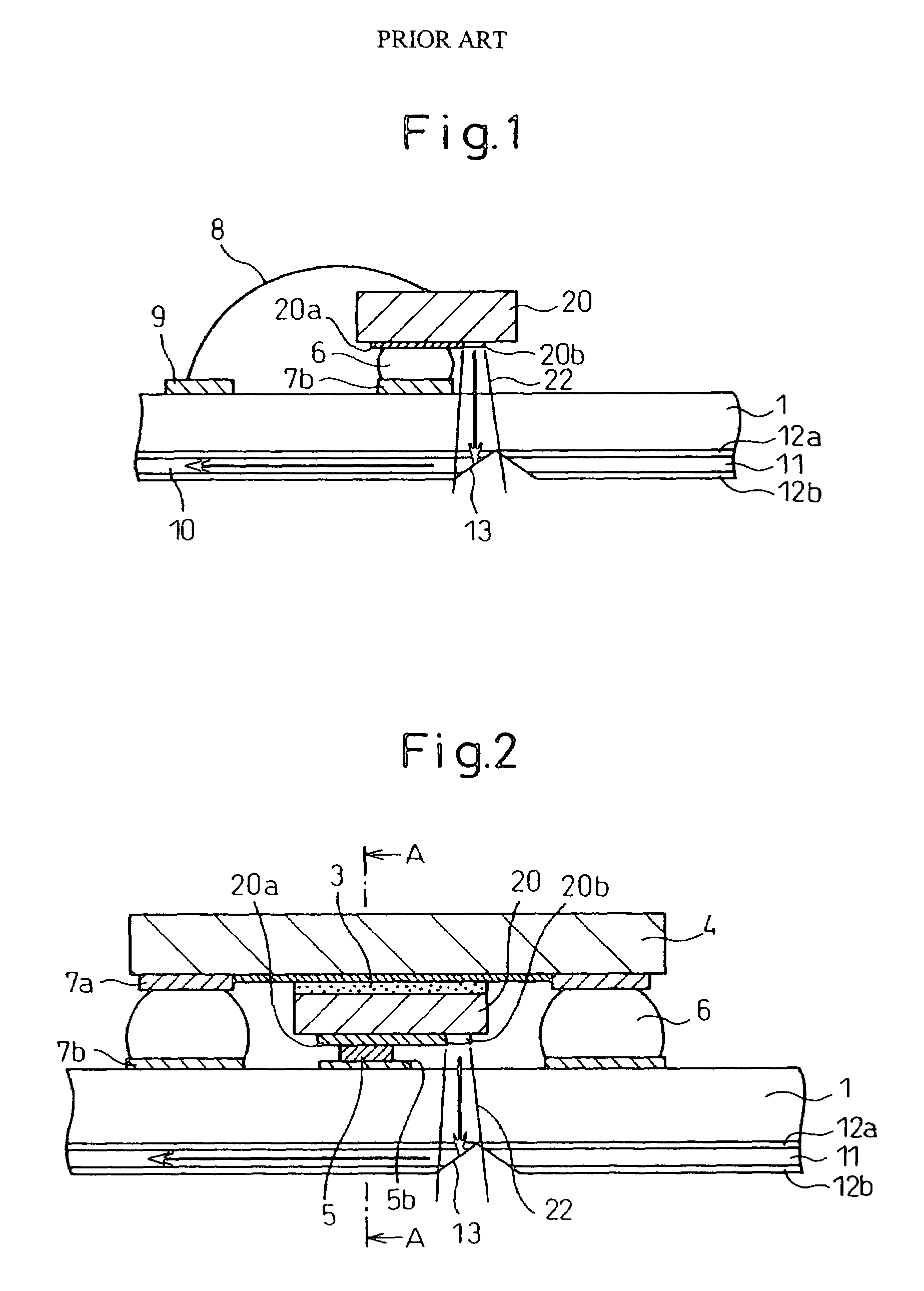
[0023]Before the explanations of the embodiments of this invention, one of comparative examples will be described.

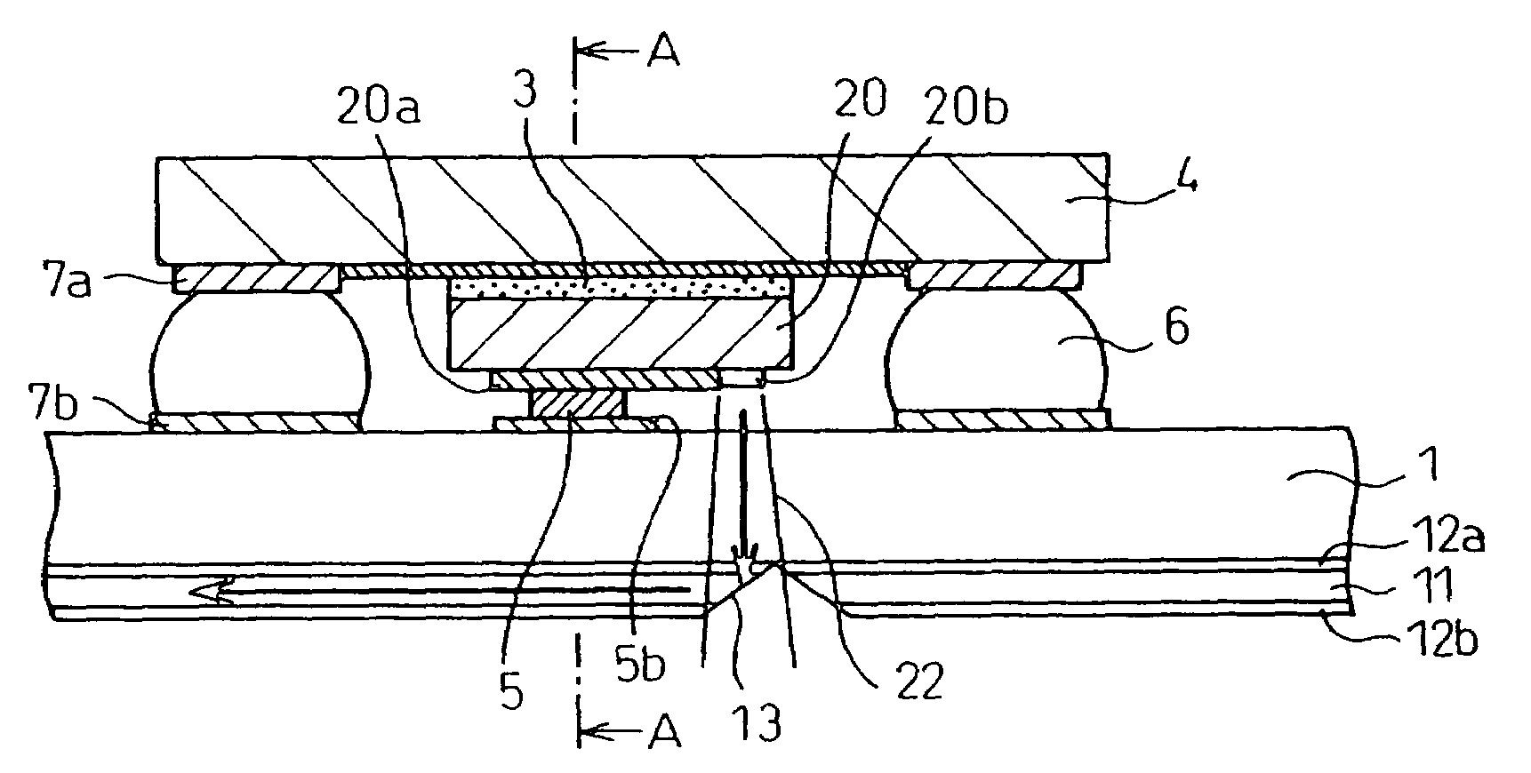
[0024]FIG. 1 is an arrangement view showing a mounting structure of a surface light emitting (light receiving) semiconductor element.

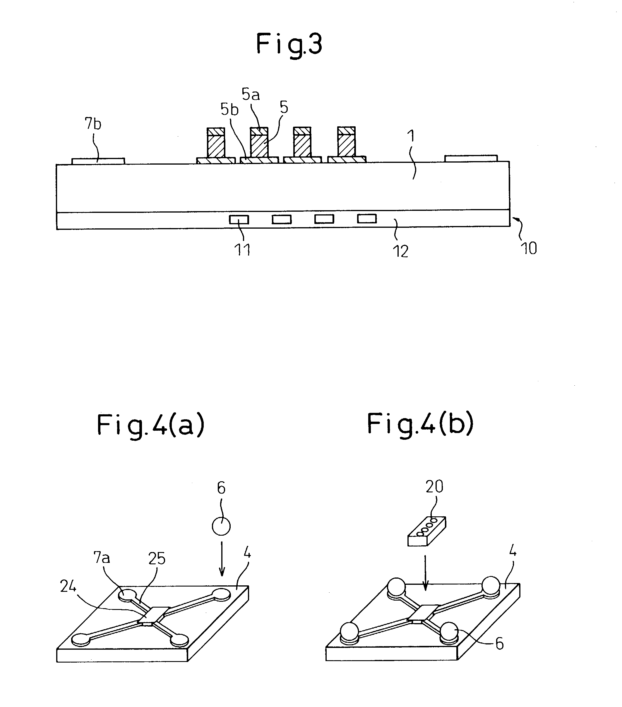
[0025]In FIG. 1, the optical wave-guide substrate 1 is composed of a glass substrate through which a laser beam can be transmitted. On one face (lower face in FIG. 1) of the optical wave-guide substrate 1, there is provided an optical wave-guide 10. The optical wave-guide 10 includes: a core 11 through which a laser beam passes; and a clad 12 (under-clad 12a and over-clad 12b) arranged around the core 11. The optical wave-guide substrate 1 is provided with a V-shaped groove mirror 13 for reflecting a laser beam.

[0026]The conventional method is described as follows. As shown in FIG. 1, the light emitting (receiving) element 20 is mou...


PUM


Abstract

It is an object of the present invention to enhance laser beam transmitting efficiency by accurately controlling an interval between a light emitting (light receiving) element (20) and an optical wave-guide substrate (1) without causing any fluctuation in the interval in a mounting structure of the light transmitting element in which the light emitting (light receiving) element (20) is mounted on the optical wave-guide substrate (1). When the light emitting (light receiving) element is joined to the sub-mount chip (4) and when the sub-mount chip (4) is joined to the optical wave-guide while the element is being directed to the substrate side, the sub-mount chip and the optical wave-guide substrate are joined to each other by the solder bump (6). A post (5) is arranged for regulating an interval between the light emitting (light receiving) element and the optical wave-guide substrate.

Description

BACKGROUND OF THE INVENTION[0001]1. Field of the Invention[0002]The present invention generally relates to an optical transmission device. More particularly, the present invention relates to a mounting structure or a printed board unit for optical transmission, and a mounting method of mounting a surface light emitting (light receiving) semiconductor element, which emits or receives a laser beam used for optical transmission, on an optical wave-guide substrate.[0003]2. Description of the Related Art[0004]The following prior art is known.[0005]Japanese Unexamined Patent Publication No. 9-26530 discloses the following technique. In an optical module in which optical elements of surface light emitting (light receiving) type and optical fibers are arranged on a plane of the same mounting substrate, the optical module having an optical coupling system, in which an optical path is converted on a side of a stationary groove of the optical fibers, in order to stabilize the characteristic an...

Claims


Application Information

Patent Timeline
Patent Type & Authority Patents(United States)
IPC IPC(8): G02B6/42G02B6/43
CPCG02B6/42G02B6/43H01L2224/48091H01L2224/73257H01L2924/00014
Inventor KANDA, TAKASHISEYAMA, KIYOTAKASUGIMOTO, KAORUOBATA, SOUICHIMAEHARA, YASUTOMO
Owner FUJITSU LTD
Why Eureka
Try Eureka