Actuated film display device

a technology of actuating film and display device, which is applied in the direction of identification means, instruments, computing, etc., can solve the problems of large number of driving ics, and achieve the effect of simple driving circui

Inactive Publication Date: 2005-11-08
PHARMACIA AB
View PDF19 Cites 29 Cited by
  • Summary
  • Abstract
  • Description
  • Claims
  • Application Information

AI Technical Summary

Benefits of technology

[0005]An object of the present invention is to provide an actuated film display device capable of displaying gray scale by a simple driving circuit.
[0031]According to the present invention, the gray scale can be displayed by the movable film display device without using numerous signal lines and scanning lines. Therefore, it is not necessary to use a large number of driving ICs for driving the numerous signal line and scanning lines. As a result, cost can be reduced. Furthermore, the display device can be reduced in size.

Problems solved by technology

However, for the gray scale display in the actuated film display device mentioned above, a large number of driving ICs are required.

Method used


Image

  • Actuated film display device
  • Actuated film display device
  • Actuated film display device

Examples


first embodiment

[0076](First Embodiment)

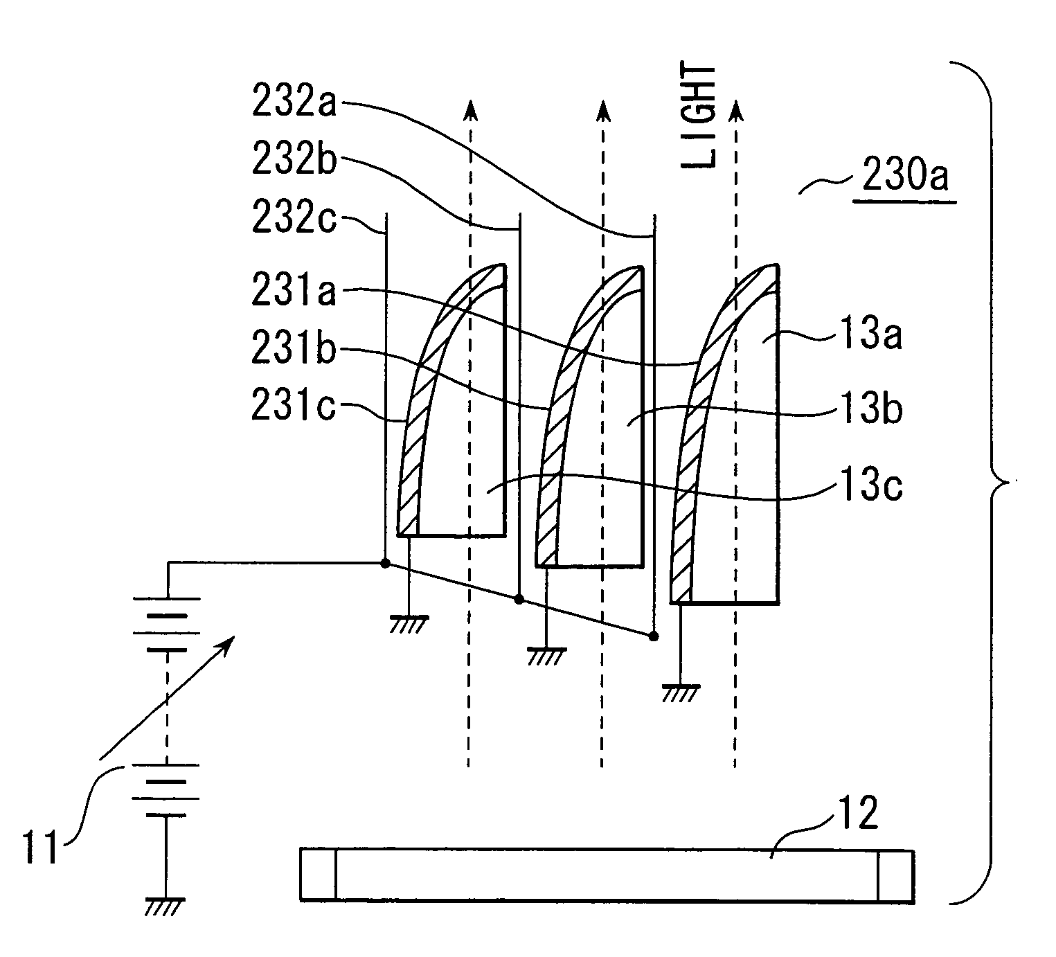
[0077]FIG. 9 shows an optical shutter set corresponding to one pixel of an actuated film display according to the first embodiment of the present invention. In the actuated film display device of this embodiment, one pixel is formed by using a shutter set 230a which is constituted of at least two shutter units different in optical distance.

[0078]In the first embodiment, three types of shutter units different in optical distance are prepared. More specifically, the shutter units have movable films different in length and transparent light guiding fixed electrode portions having length values corresponding to the movable films. Each of the transparent light guiding fixed electrode portions 231a–231c is, for example, grounded. The same voltage is applied to the movable film electrodes 232a–232c different in length by a variable voltage power source 11. Furthermore, a fluorescent light is used as a light source 12. The light from the light source 12 passes throug...

second embodiment

[0086](Second Embodiment)

[0087]FIG. 12 is a schematic cross-sectional view of a shutter set corresponding to one pixel of the actuated film display device according to the second embodiment of the present invention.

[0088]The actuated film display device of the second embodiment is the same as that of the first embodiment in that a plurality of movable film shutter units are arranged in one pixel but differs in that one pixel is formed by using movable film shutter units which have the movable film electrodes of at least two type of thicknesses.

[0089]As shown in FIG. 12, in the shutter set 230b of the second embodiment, wiring of transparent light guiding fixed electrode portions 231a′–231c′, transparent light guiding bodies 13a′–13c′, and movable film electrodes 232a′–232c′ is carried out in the same manner as in the first embodiment. The wiring may be formed of the same material in the first embodiment.

[0090]However, all movable film shutter units of the actuated film display devic...

third embodiment

[0094](Third Embodiment)

[0095]FIG. 13 is a schematic cross-sectional view of a shutter set corresponding to one pixel of the actuated film display device according to a third embodiment of the present invention.

[0096]The actuated film display device of the third embodiment is the same as that of the first embodiment in that a plurality of movable film shutter units are arranged in one pixel but differs in that there are at least two kind of distances between the transparent light guiding fixed electrode portion and a fixed end of the movable film electrode in one pixel.

[0097]As shown in FIG. 13, in the shutter set 230c of the third embodiment, wiring of transparent light guiding fixed electrode portions 231a′–231c′ and transparent light guiding bodies 13a′–13c′ is carried out in the same manner as in the first embodiment. The wiring may be formed of the same material as in the first embodiment.

[0098]However, all the shutter units of the actuated film display device of the third embo...


PUM

PropertyMeasurementUnit
thicknessaaaaaaaaaa
thicknessaaaaaaaaaa
thicknessaaaaaaaaaa

Abstract

An actuated film display device comprises a first fixed electrode, a first movable film electrode, which is placed to face the first fixed electrode to form a first optical path on an opposing side to the first fixed electrode, and which has a fixed end and a movable end, the movable end being displaced toward the first fixed electrode by application of a first potential difference between the first fixed electrode and the first movable film electrode, thereby shutting off the first optical path, a second fixed electrode placed at a predetermined distance from the first fixed electrode, and a second movable film electrode, which is placed to face the second fixed electrode to form a second optical path on an opposing side to the second fixed electrode, which has a fixed end and a movable end, the movable end being displaced toward the second fixed electrode by application of a second potential difference between the second fixed electrode and the second movable film electrode, thereby shutting off the second optical path. The display device having the above-described optical shutter as one pixel can display gray scale without using numerous signal lines and scanning lines.

Description

CROSS-REFERENCE TO RELATED APPLICATIONS[0001]This application is a Continuation of U.S. patent application Ser. No. 09 / 651,024 filed Aug. 30, 2000, now U.S. Pat No. 6,618,034 and is based upon and claims the benefit of priority from the prior Japanese Patent Application No. 11-274004, filed Sep. 28, 1999, the entire contents of these applications are incorporated herein by reference.BACKGROUND OF THE INVENTION[0002]The present invention relates to an actuated film display device.[0003]In large display devices and portable display devices, it has recently been desired that the power consumption is lowered. As the display device attaining the low power consumption, known is an actuated film display device using a movable film shutter in which a movable film is driven by an electrostatic force.[0004]The fundamental structure of the actuated film display device is disclosed in Japanese Patent Application Publicatrion No. 11-95693 U.S. Pat. No. 6,239,777 B1), the contents of which are in...

Claims


Application Information

Patent Timeline
Patent Type & Authority Patents(United States)
IPC IPC(8): G09F9/37G02F1/015G02B26/08
CPCG09F9/372G02F1/015
Inventor SUGAHARA, ATSUSHILANG, RICHARD
Owner PHARMACIA AB
Why Eureka
Try Eureka