
Prefabricated and attached interconnect structure

a technology of interconnect structure and prefabricated structure, which is applied in the direction of electrical testing, measurement devices, instruments, etc., can solve the problems of high labor intensity, high cost and complexity of assembly, and the inability to fabricate spring-like interconnect structures directly on the face of larger structures, so as to achieve the effect of substantially eliminating the bending momentum in the attachment fa

Inactive Publication Date: 2005-11-15
SV PROBE PTE LTD
View PDF47 Cites 50 Cited by
  • Summary
  • Abstract
  • Description
  • Claims
  • Application Information

AI Technical Summary

Benefits of technology

This solution simplifies the assembly process, reduces fabrication complexity, and enhances the structural interlocking between the interconnect structures and the larger structure, enabling efficient and reliable electrical contact while minimizing delamination risks and maintaining cost-effectiveness.

Problems solved by technology

Secondly, the interconnect structures needs to scratch along the terminal's surface to remove any eventual insulating oxides and films prior to establishing a conductive contact to the test terminals.
Thirdly, the interconnect structures must be simple in shape and configuration to be cost effectively fabricated in high numbers.
Unfortunately, the buckling beams need to be held at both ends with sufficient lateral space to permit buckling in the middle of the buckling beams.
This results in a relative complicate and cost intensive assembly.
Unfortunately, the effort for fabricating spring like interconnect structures directly on the face of a larger structure is relatively high.
Also, since the deflection of each spring like structure is opposed by the larger structure, each interface between the two of them may be exposed to high stresses.
As a result, the interface may need additional structural support.
In the prior art, complicated fabrication steps are performed for fabricating spring like interconnect structures.
In the prior art, several problems associated with the fabrication of small scale interconnect structures directly on the face of a larger structure remain unresolved.
One problem is to position and transport the miniature structure during its fabrication.
A second problem is to precisely position an eventually pre-fabricated structure in its final assembly position on a larger structure.
A third problem is to attach the eventually pre-fabricated structure in its final assembly position.
The attachment is particularly problematic, where stresses are at a maximum in the attachment interface.

Method used


Image

  • Prefabricated and attached interconnect structure
  • Prefabricated and attached interconnect structure
  • Prefabricated and attached interconnect structure

Examples


Embodiment Construction

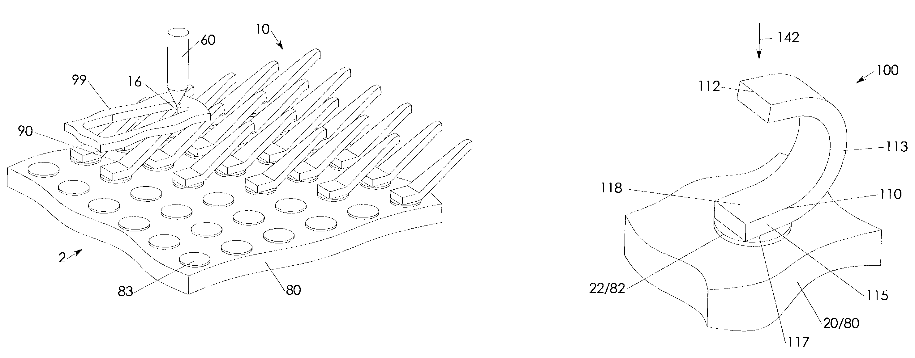
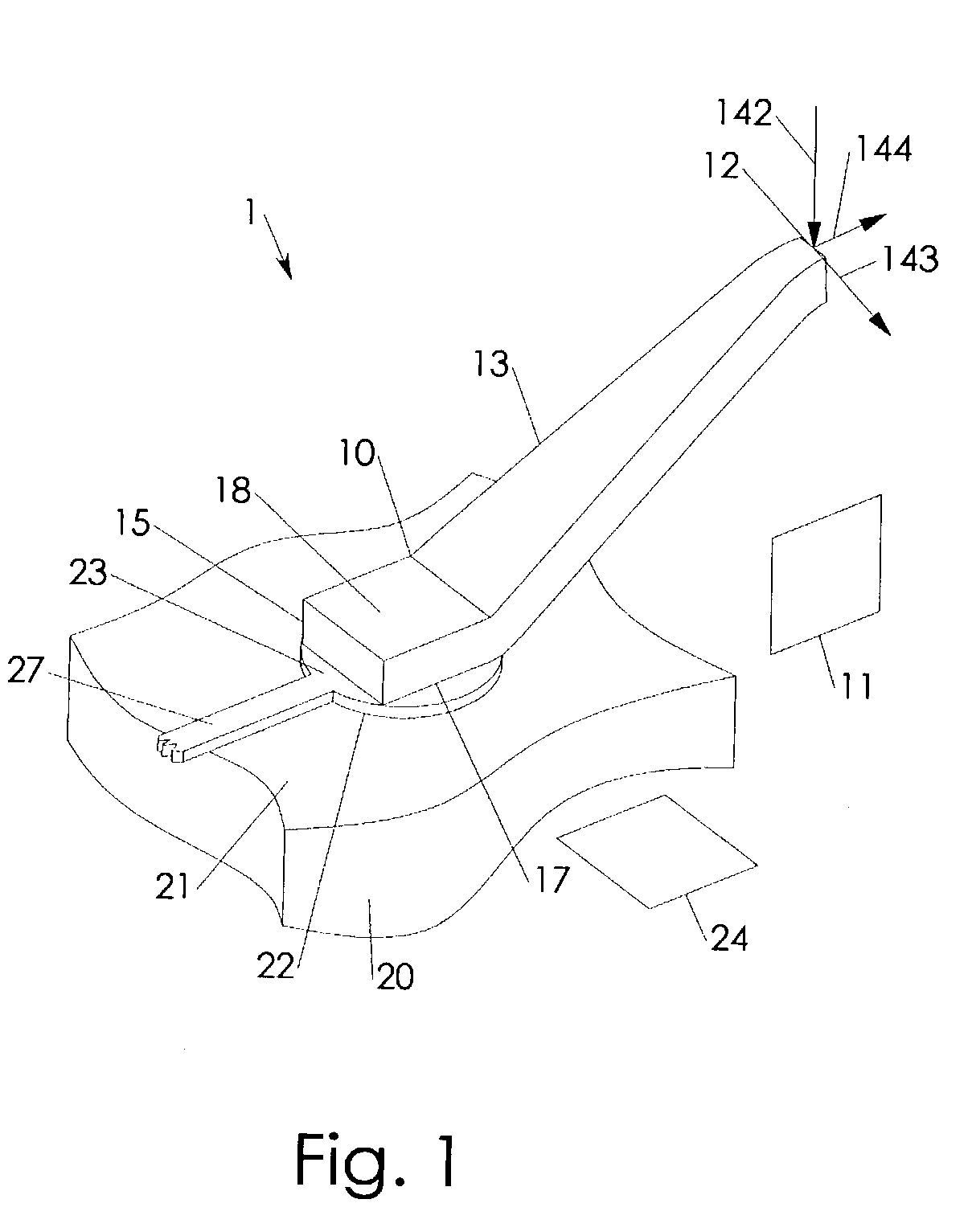
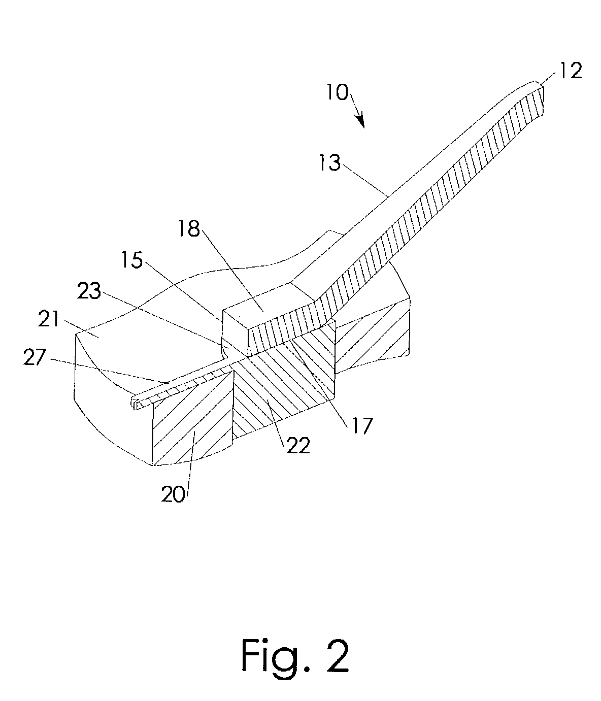
[0035]As shown in FIG. 1 and according to a first embodiment of the invention, an interconnect assembly 1 includes a prefabricated interconnect structure 10 attached to a conductive terminal 22 accessible on a face 21 of the larger structure 20. Prior to attachment, the interconnect structure 10 is prefabricated with an attachment base 15, a suspension element 13 and a contacting end 12. The attachment base 15 has an access face 18 and an attachment face 17 that substantially opposes the access face 18.

[0036]Rigid connection between the interconnect structure 10 and the attachment terminal 22 is provided by metallurgical bonding in an attachment interface between the attachment face 17 and a terminal face 23. Metallurgical bonding in context with the present invention includes soldering, brazing and welding. The metallurgical bonding provides a connection that is electrically conductive and structurally substantially rigid opposing at least a bending stress resulting in the attachme...


PUM

PropertyMeasurementUnit
electrically conductiveaaaaaaaaaa
conductiveaaaaaaaaaa
electricaaaaaaaaaa

Abstract

A interconnect assembly features a prefabricated interconnect structure metallurgically bonded to a terminal of a larger structure. Fabrication of the interconnect structure's independently and seperate from the larger structure enables the use of economic mass fabrication techniques that are well-known for miniature scale sheet metal parts. During fabrication, positioning and attachment, each interconnect structure is combined with and / or held in a carrier structure from which it is separated after attachment to the terminal. The interconnect structure is configured such that an attachment tool may be brought into close proximity to the attachment interface between the interconnect structure and the terminal for a short and direct transmission of bonding energy onto the attachment interface. The attachment interface provides for an electrically conductive and a bending stress opposing mechanical connection between the interconnect structure and the terminal. The interconnect assembly is preferably part of a probe apparatus.

Description

FIELD OF INVENTION[0001]The present invention relates to interconnect structures for conductively contacting terminals. Particularly, the present invention relates to interconnect structures of a probe apparatus for testing semiconductor devices.BACKGROUND OF INVENTION[0002]A conventional probe apparatus for testing semiconductor devices includes a number of interconnect structures for temporarily contacting test terminals of the tested device. As the semiconductor technology advances, the tested devices become increasingly smaller while the number of simultaneously accessed terminals continues to increase. At the same time, commercial competition forces the industry to provide semiconductor testing at ever decreasing cost. To meet these demands, there exists a need for further improvement of probe apparatus.[0003]A crucial component in a probe apparatus are the interconnect structures that are tightly arrayed within a probe apparatus. The interconnect structures are configured for ...

Claims


Application Information

Patent Timeline
Patent Type & Authority Patents(United States)
IPC IPC(8): G01R1/073
CPCG01R1/07357Y10T29/49117
Inventor KISTER, JANUARYBEATSON, DAVIDLAURENT, EDWARD
Owner SV PROBE PTE LTD
Learn More