Device and method for compensating non-uniformities in imaging systems

a technology of non-uniformity and imaging system, applied in the field of exposure and modulation, can solve the problems of non-uniformity in the light modulator, the inability of the human eye to detect the differences between adjacent pixels of photosensitive materials, and the inability to compensate, so as to achieve the effect of optimizing the quality of the exposur

Inactive Publication Date: 2005-11-15
XEIKON PREPRESS NV
View PDF7 Cites 43 Cited by
  • Summary
  • Abstract
  • Description
  • Claims
  • Application Information

AI Technical Summary

Benefits of technology

[0006]The object of the invention, therefore, is to present a device and a method with which the exposure quality can be optimized using simple means.

Problems solved by technology

The problem with the device described is that non-uniformities in the light modulator, e.g., caused by differences in illumination or imaging power differing at the local level when cells are controlled in uniform fashion, produce different exposure results within a partial image on the material to be exposed.
As a rule, the differences between adjacent pixels on the photosensitive material cannot be detected by the human eye, because humans primarily see differences.
Compensation is very problematic in areas, in particular, where non-adjacent pixels are projected next to each other on the photosensitive material.
Attempts to transfer the system for compensating non-uniformities used in the DSI system to adjust the energy in each cell separately were not successful.

Method used


Image

  • Device and method for compensating non-uniformities in imaging systems
  • Device and method for compensating non-uniformities in imaging systems
  • Device and method for compensating non-uniformities in imaging systems

Examples


Embodiment Construction

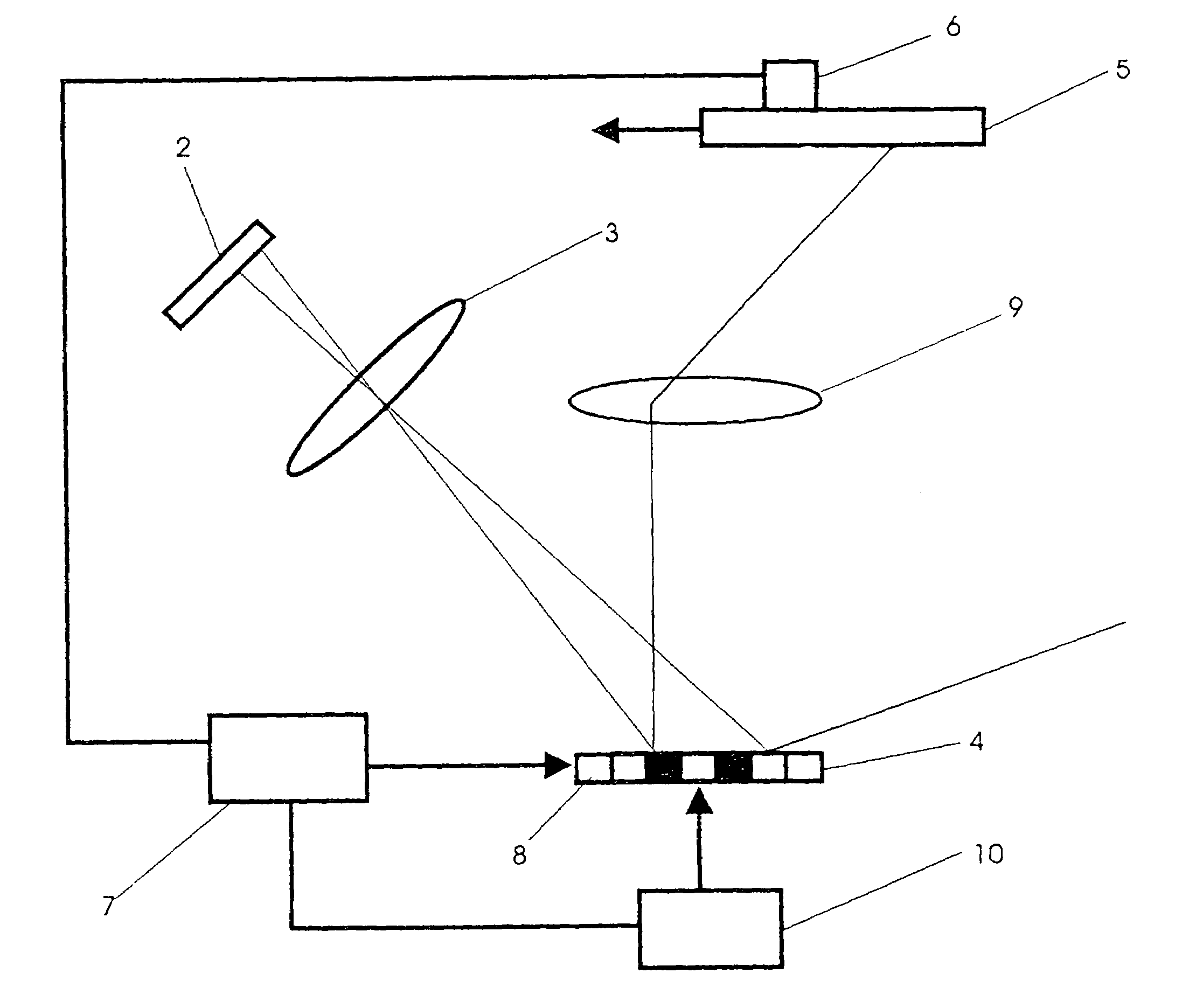
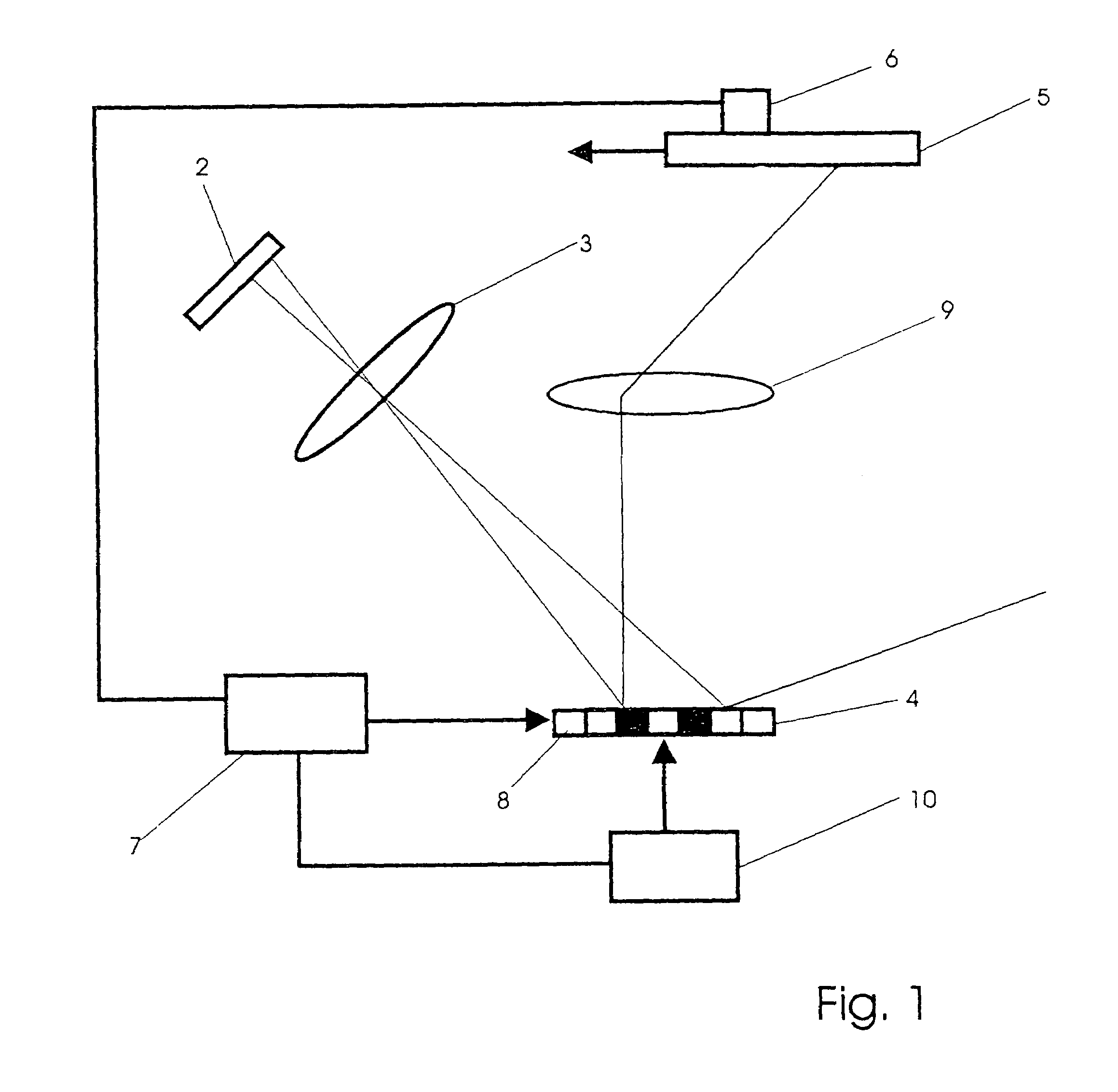
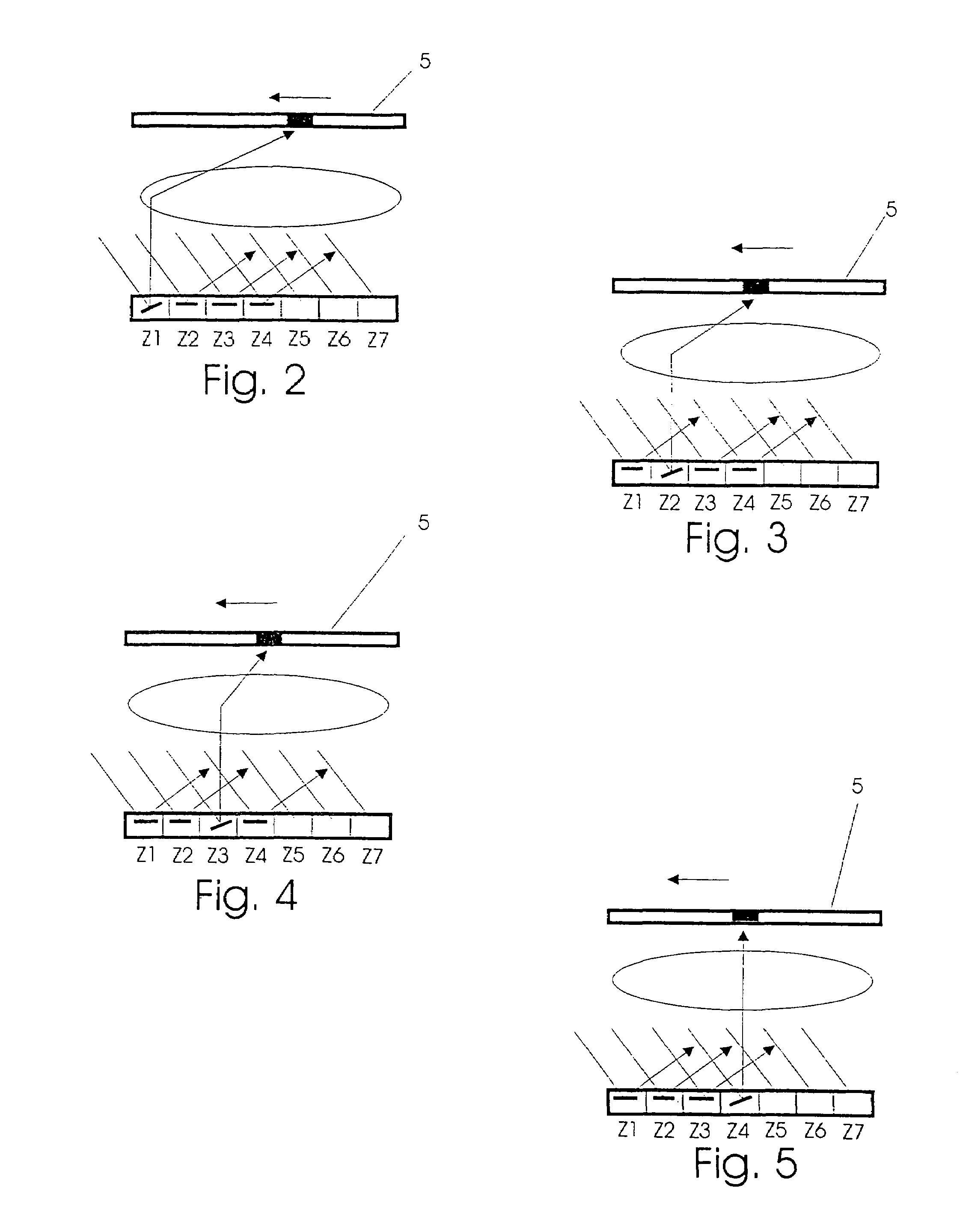
[0019]FIG. 1 is a schematic drawing of the exposure and modulation device 1: a light source 2 is imaged on a light modulator 4 using a first lens 3. The position of the photosensitive material 5 relative to the light modulator 4 is changed by a locator 6. The relative motion takes place in the direction of the cells of a row of the light modulator. Data patterns are transferred to the first column with cells 8 of the light modulator using a driver circuit 7. It is important that the transmission of the data pattern be synchronized with the motion of the photosensitive material 5. The data pattern transferred to the first column is moved to the next column in synchronization with the relative motion, so that the data pattern transferred to the photosensitive material 5 remains stationary on it. The light modulator 4 comprises a plurality of columns of cells 8. The data pattern transferred to the light modulator 4 comprises combinations of activated and non-activated cells 8. If the c...


PUM

PropertyMeasurementUnit
scrolling frequencyaaaaaaaaaa
photosensitiveaaaaaaaaaa
speedaaaaaaaaaa

Abstract

An illumination and modulation device is described, as well as a method for modulating the exposure intensity in the integrating digital screen imaging system (IDSI), comprising a light source, a light modulator, and various devices. The object of the invention is to present a device and a method with which the exposure quality can be optimized using simple means. The object on which the invention is based is attained by the fact that the device comprises at least one device for varying the number of cells of the light modulator used to expose the photosensitive material or by the fact that, in the method according to the invention, the number of cells of the light modulator used to expose the photosensitive material can be varied.

Description

BACKGROUND OF THE INVENTION[0001]The invention concerns an exposure and modulation device for modulating the exposure intensity in the integrating digital screen imaging system (IDSI) comprising a light source and a light modulator that has a plurality of rows of light-modulating cells, and comprising a device for imaging on the light modulator, a device for imaging the light modulator onto photosensitive material, and a device for producing a relative motion between the light modulator and the photosensitive material, whereby the direction of motion is basically perpendicular to the direction of the rows of light-modulating cells, and comprising a device for scrolling a data pattern through the various columns of the light modulator at a speed by means of which the imaging of any data pattern is kept basically stationary relative to the photosensitive material during the motion.[0002]The invention further concerns a method for exposing and modulating the exposure intensity in the i...

Claims


Application Information

Patent Timeline
Patent Type & Authority Patents(United States)
IPC IPC(8): B41J2/435B41J2/465B41J2/52G02B26/08G06K15/12B41J2/445G02F1/03G02F1/09G02F1/13G02F1/31G03B27/32
CPCB41J2/465B41J2/52G02B26/0833G02B26/085G06K15/1252G09G3/34
Inventor EGGERS, STEFANANDREAE, CLAAS
Owner XEIKON PREPRESS NV
Why Eureka
Try Eureka