Chip fabrication procedure and simulation method for chip testing with performance pre-testing

Inactive Publication Date: 2005-11-15
VIA TECH INC
View PDF17 Cites 0 Cited by
  • Summary
  • Abstract
  • Description
  • Claims
  • Application Information

AI Technical Summary

Benefits of technology

[0008]Accordingly, it is the primary object of the present invention to provide a chip fabrication procedure with performance pre-testing, in which the chip is produced after a simulation on design validity and product performance is carried out so as to confirm the product advantage.
[0009]It is a secondary object of the present invention to provide a chip fabrication procedure with performance pre-testing, in which the simulation is carried out in a software-based simulation environment so as to prevent the waste of raw materials.

Problems solved by technology

Therefore, product testing has become an important issue for the manufacturers.
However, the fore-mentioned procedure does not guarantee that the thus produced chip has expected performance.
It may take a relatively long time.
Moreover, if the performance fails to meet the standards after being tested, the cost as well as the efforts according to the fabrication procedure would be in vain.
As a result, the thus increased cost will make the product less competitive in the market.

Method used


Image

  • Chip fabrication procedure and simulation method for chip testing with performance pre-testing
  • Chip fabrication procedure and simulation method for chip testing with performance pre-testing
  • Chip fabrication procedure and simulation method for chip testing with performance pre-testing

Examples


Embodiment Construction

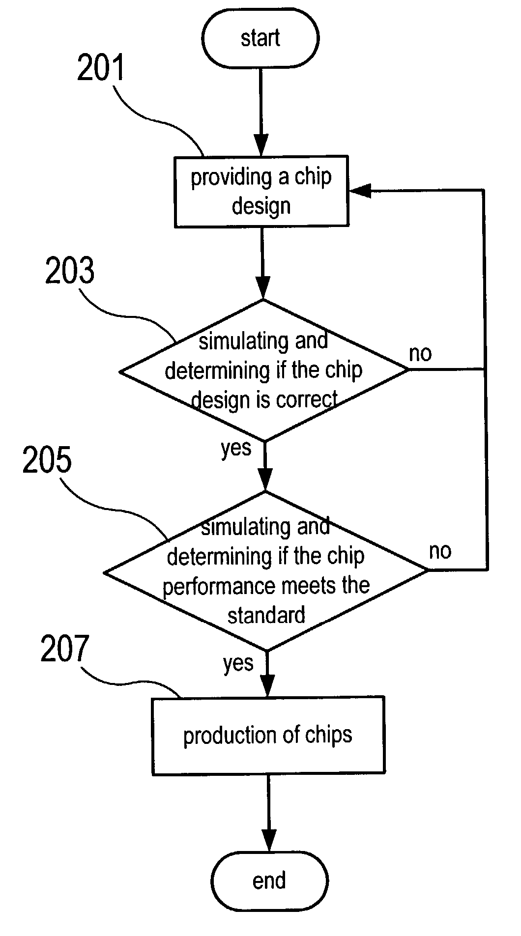
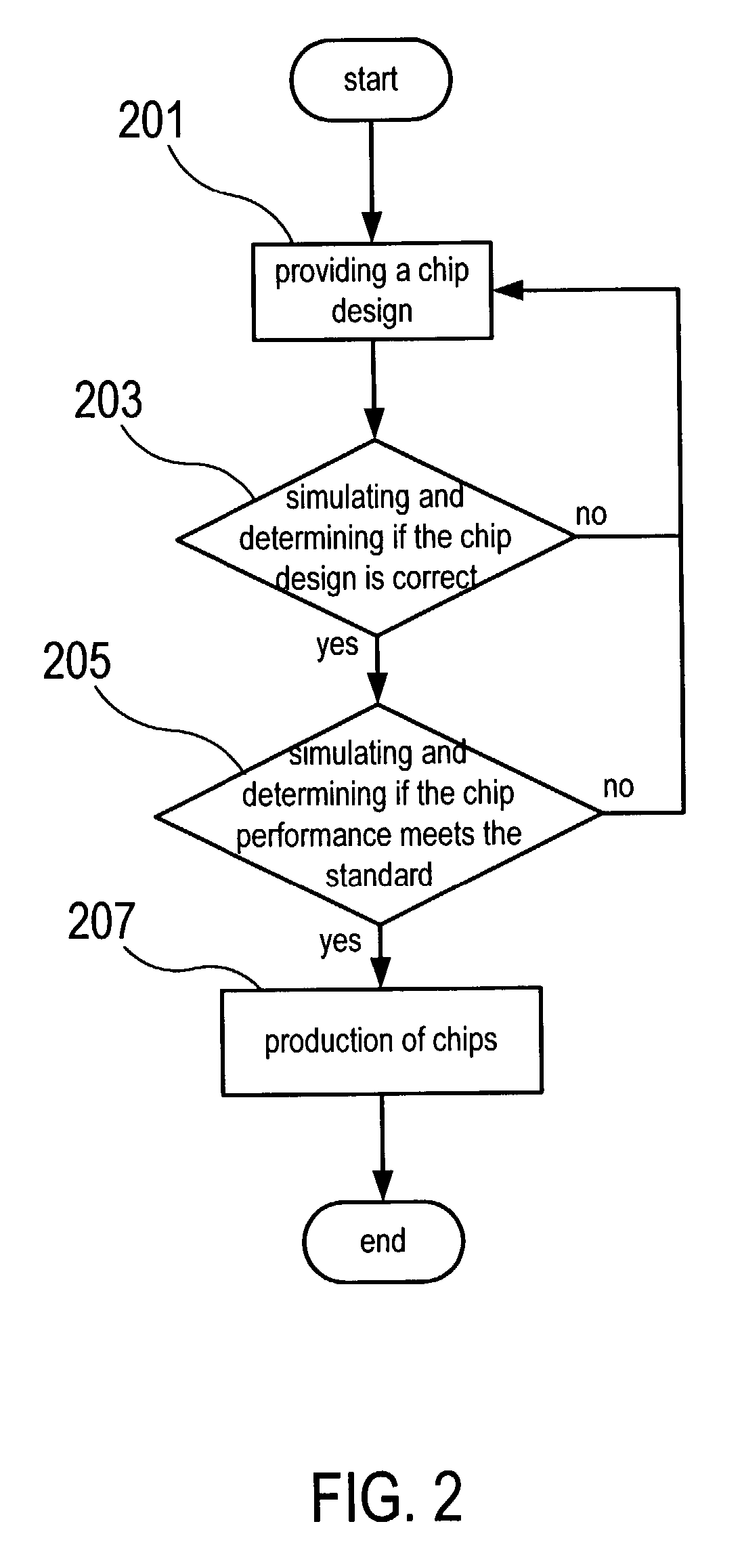
[0020]The present invention providing a chip fabrication procedure as well as a simulation method for chip testing with performance pre-testing can be exemplified by the preferred embodiment as described hereinafter.

[0021]First of all, please refer to FIG. 2, which is a flow chart showing a chip fabrication procedure in accordance with one preferred embodiment of the present invention. As shown in the figure, the procedure begins with step 201, in which a chip design is provided. The chip design is tested in a simulation environment, and whether the chip design responds correctly to various testing commands is determined (step 203). If the chip design does not respond correctly to the testing commands, the procedure returns to step 201 for modifying the chip design. On the contrary, if the chip design responds correctly to the testing commands, the procedure proceeds with step 205, in which the performance of the chip design is examined to determine if the performance meets the pre-...


PUM


Abstract

The present invention discloses a chip fabrication procedure as well as a simulation method for chip testing with performance pre-testing. The chip fabrication procedure with performance pre-testing comprising steps of: providing a chip design; determining if the chip design is correct by using a simulation environment; determining if the chip performance meets the standards by using a performance testing process; and proceeding with production of chips. The simulation method for chip testing comprises steps of: providing a simulation environment corresponding to a chip design; providing at least one set of testing commands; executing the testing commands; and calculating the time required for completing executing the testing commands. The present invention is advantageous since the time requited for product testing is reduced and so is the fabrication cost.

Description

BACKGROUND OF THE INVENTION[0001]1. Field of the Invention[0002]The present invention generally relates to a chip fabrication procedure and, more particularly, to a chip fabrication procedure as well as a simulation method for chip testing with performance pre-testing, in which the chip is produced after a simulation on design validity and product performance is carried out so as to confirm the product advantage, such that the time requited for product testing is reduced and so is the fabrication cost.[0003]2. Description of the Prior Art[0004]In recent years, with the high development in electronic- and information-related industries, people have increasing needs for better performance of various electronic and information products. In view of this, the industries have made lots of efforts to develop various new products. These new products may, however, cooperate with different specifications from the conventional ones. It is inevitable that the new products with various specifica...

Claims


Application Information

Patent Timeline
IPC IPC(8): G01R31/3185G01R31/28G01R31/3183G06F17/50
CPCG01R31/318357G01R31/318505G06F17/5022G06F30/33
Inventor WEN, FUCHUHAN, TONYHSIAO, CHIN-FA
Owner VIA TECH INC
Why Eureka
Try Eureka