
Lateral diode with multiple spacers

a diode and spacer technology, applied in the field of diodes, can solve the problems of limiting the operating voltage and ambient temperature environment of the chip, special challenges in the electrical performance windows of the integrated circuit, and restricting the performance of the circuit, so as to reduce the width of the second spacer structure

Active Publication Date: 2005-11-22
GLOBALFOUNDRIES US INC
View PDF6 Cites 41 Cited by
  • Summary
  • Abstract
  • Description
  • Claims
  • Application Information

AI Technical Summary

Benefits of technology

[0011]In accordance with another aspect of the present invention, a method of manufacturing a diode is provided that includes forming a gate structure on a semiconductor portion of a substrate. The semiconductor portion has a first conductivity type. First and second spacer structures are formed on opposite sides of the gate structure. A first impurity region of a second conductivity type is formed proximate the first spacer structure while the semiconductor portion lateral to the second spacer structure is masked. The first impurity region and the semiconductor portion defined a pn junction. A width of the second spacer structure is reduced the second spacer structure and the first impurity region are masked. A second impurity region of the first conductivity type is formed in the semiconductor portion proximate the second spacer structure but in spaced-apart relation to the pn junction.

Problems solved by technology

However, the microscopic geometries and tight electrical performance windows of integrated circuits present special challenges.
Elevated chip operating temperatures impose constraints on the performance of the circuit in several ways.
Furthermore, higher operating temperatures restrict the permissible operating voltage and ambient temperature environment of the chip.
Lastly, chip life span is adversely impacted by higher operating temperatures.
If the available mechanisms for integrated circuit heat dissipation cannot adequately handle the I2R heat propagation, compromises in the speed performance, the operating voltage, the applications and the design life span of the integrated circuit may have to be made.
In addition, in a bulk silicon device, the depth of the silicon body is such that the resistance thereof is relatively low such that errors introduced due to series resistance may be managed.
The migration to semiconductor-on-insulator technology has introduced a set of challenges associated with implementing thermal on-chip diodes.
The higher series resistances can adversely affect the accuracy of the temperature readings from the diode.

Method used


Image

  • Lateral diode with multiple spacers
  • Lateral diode with multiple spacers
  • Lateral diode with multiple spacers

Examples


Embodiment Construction

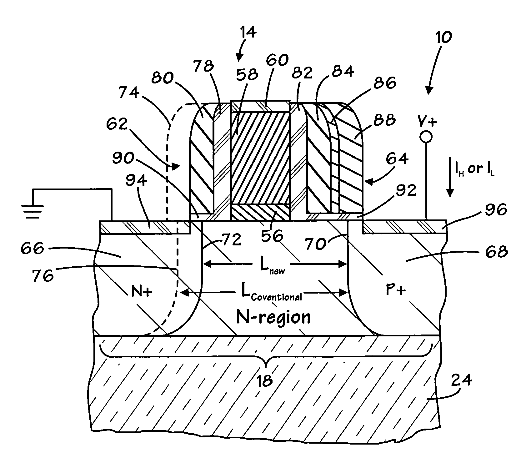
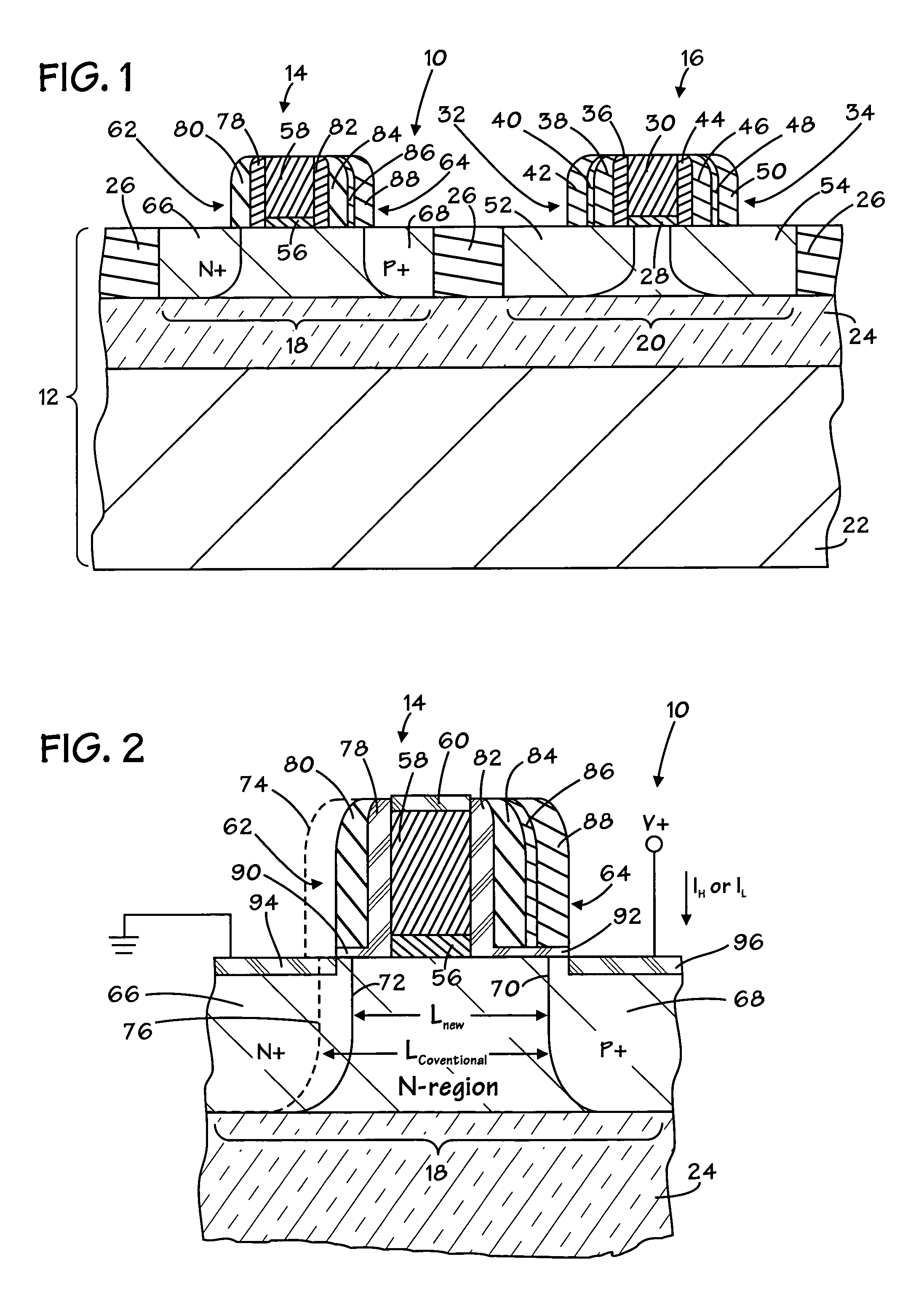
[0020]In the drawings described below, reference numerals are generally repeated where identical elements appear in more than one figure. Turning now to the drawings, and in particular to FIG. 1, therein is depicted a cross-sectional view of an exemplary embodiment of an integrated circuit 10 implemented on a substrate 12. In an exemplary embodiment, the substrate is a semiconductor-on-insulator substrate. However, other substrates useful for integrated circuit fabrication may be used. The integrated circuit 10 consists of numerous circuit devices, two of which are shown and numbered 14 and 16. In an exemplary embodiment, the circuit device 14 is a diode and the circuit device 16 is a transistor. The circuit device 16 may be virtually any type of circuit device used in an integrated circuit. The diode 14 and the transistor 16 are implemented on respective active regions 18 and 20 that are composed of a suitable semiconductor substrate material, such as, for example, silicon, germani...


PUM


Abstract

Various circuit devices, including diodes, and methods manufacturing therefor are provided. In one aspect, a method manufacturing is provided that includes forming a gate structure on a semiconductor portion of a substrate. The semiconductor portion has a first conductivity type. First and spacer structures are formed on opposite sides of the gate structure. A first impurity region of a second conductivity type is formed proximate the first spacer structure while the semiconductor portion lateral to the second spacer structure is masked. The first impurity region and the semiconductor portion define a junction. A width of the second spacer structure is reduced while the second spacer structure and the first impurity region are masked. A second impurity region of the first conductivity type is formed in the semiconductor portion proximate the second spacer structure. The method provides a diode with reduced series resistance.

Description

BACKGROUND OF THE INVENTION[0001]1. Field of the Invention[0002]This invention relates generally to semiconductor processing, and more particularly to diodes and methods of making the same.[0003]2. Description of the Related Art[0004]Heat management plays a vital role in the process of designing most electrical devices. However, the microscopic geometries and tight electrical performance windows of integrated circuits present special challenges. Elevated chip operating temperatures impose constraints on the performance of the circuit in several ways. Chip operating temperature has a direct impact on the maximum available clocking speed and thus the overall speed performance of the integrated circuit. Furthermore, higher operating temperatures restrict the permissible operating voltage and ambient temperature environment of the chip. Lastly, chip life span is adversely impacted by higher operating temperatures. If the available mechanisms for integrated circuit heat dissipation canno...

Claims


Application Information

Patent Timeline
Patent Type & Authority Patents(United States)
IPC IPC(8): H01L29/76H01L29/66H01L27/06H01L27/08H01L29/739
CPCH01L27/0629H01L27/0814H01L29/7391
Inventor BULLER, JAMES F.
Owner GLOBALFOUNDRIES US INC
Features
  • Generate Ideas
  • Intellectual Property
  • Life Sciences
  • Materials
  • Tech Scout
  • Unparalleled Data Quality
  • Higher Quality Content
  • 60% Fewer Hallucinations
Learn More