Memory trouble relief circuit

a memory trouble and circuit technology, applied in the field of memory trouble relief circuits, can solve the problem of inconvenient generation of leakage current even in the unused circuit, and achieve the effect of reducing the leakage current generated in the unused redundancy circuit and replacing reliably

Inactive Publication Date: 2005-11-22
PANASONIC CORP
View PDF8 Cites 71 Cited by
  • Summary
  • Abstract
  • Description
  • Claims
  • Application Information

AI Technical Summary

Benefits of technology

[0006]The present invention is designed to solve the usual problem as described above, and aimed to provide a memory trouble relief circuit which can reduce the leakage current generated by unused redundancy circuit.
[0007]A first aspect of the memory trouble relief circuit of the invention is directed to a memory trouble relief circuit for relieving the failure of a memory of a semiconductor integrated circuit having the memory, comprising: a redundancy relief circuit having a redundancy circuit by which the defective part of the memory is replaced based on the diagnosed result of the memory; and a power line of different system from that of a power source for the semiconductor integrated circuit. According to this structure, the power sources of the semiconductor integrated circuit and redundancy relief circuit are provided in separate systems. Thereby, when the memory has no failure upon inspection of the semiconductor integrated circuit, it becomes possible not to supply power to the redundancy relief circuit. Thus, a leakage current generated in an unused redundancy circuit can be reduced.
[0008]A second aspect of the memory trouble relief circuit of the invention is directed to a memory trouble relief circuit for relieving the failure of a memory of a semiconductor integrated circuit having the memory, said memory trouble relief circuit comprising: a self-diagnosis circuit for diagnosing the memory and outputting the diagnosed result to an external power control circuit and a redundancy relief circuit having a redundancy circuit by which the defective part of the memory is replaced based on the diagnosed result, wherein the supply of power to the redundancy relief circuit is controlled independently of the supply of power to the semiconductor integrated circuit by the power control circuit operating based on the diagnosed result According to this structure, based on the self-diagnosis result, the supply of power to the redundancy relief circuit is controlled independently of the supply of power to the semiconductor integrated circuit. Therefore, when the memory has no failure upon inspection of the semiconductor integrated circuit, control is exercised so as not to supply power to the redundancy relief circuit. Thereby, the leakage current generated in the unused redundancy circuit can be reduced.

Problems solved by technology

However, in the usual semiconductor including the semiconductor storage device, when the defect is not detected in the semiconductor storage device part upon inspection, a redundancy relief circuit is not used, so that leakage current is inconveniently generated even in the unused circuit.

Method used


Image

  • Memory trouble relief circuit
  • Memory trouble relief circuit
  • Memory trouble relief circuit

Examples


first embodiment

(First Embodiment)

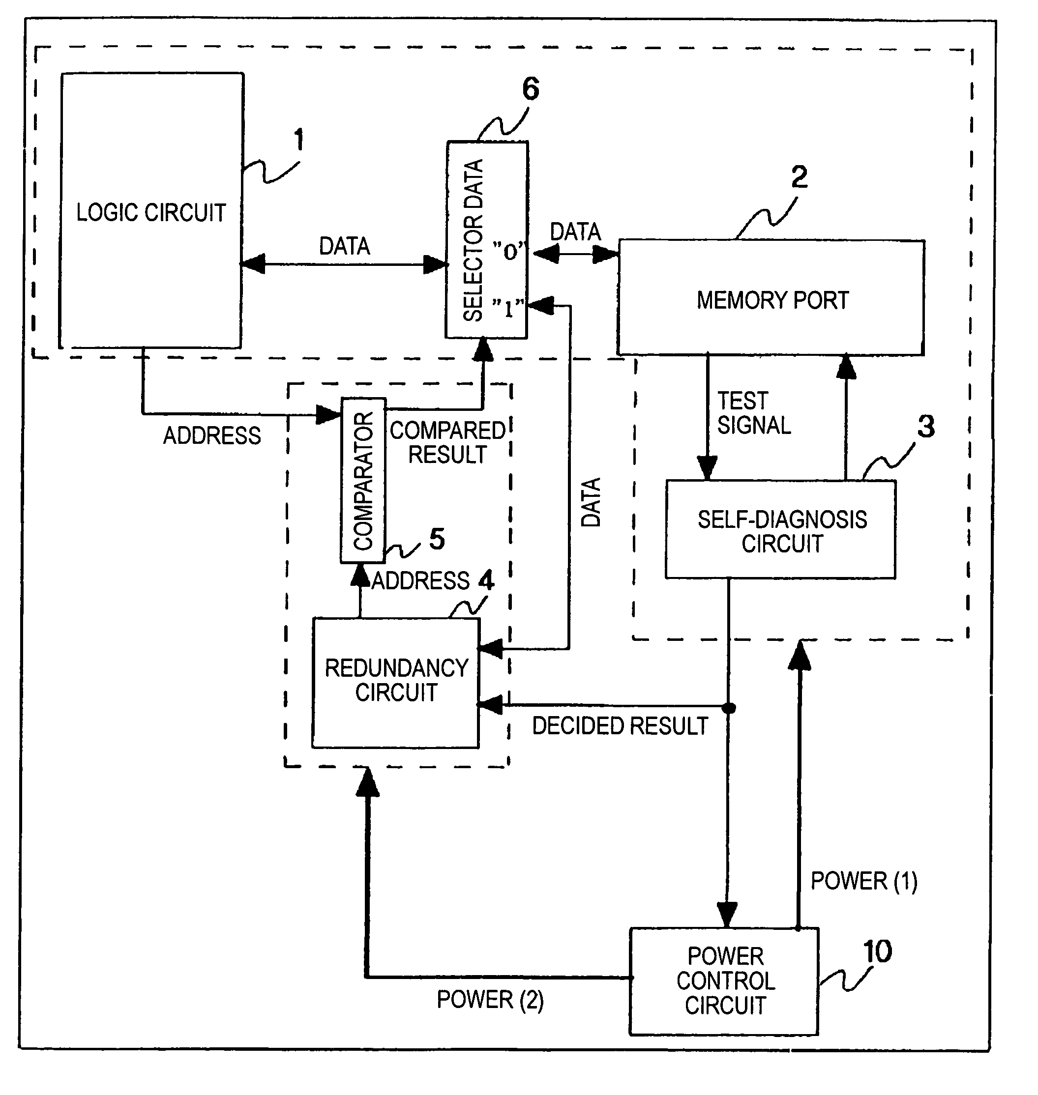
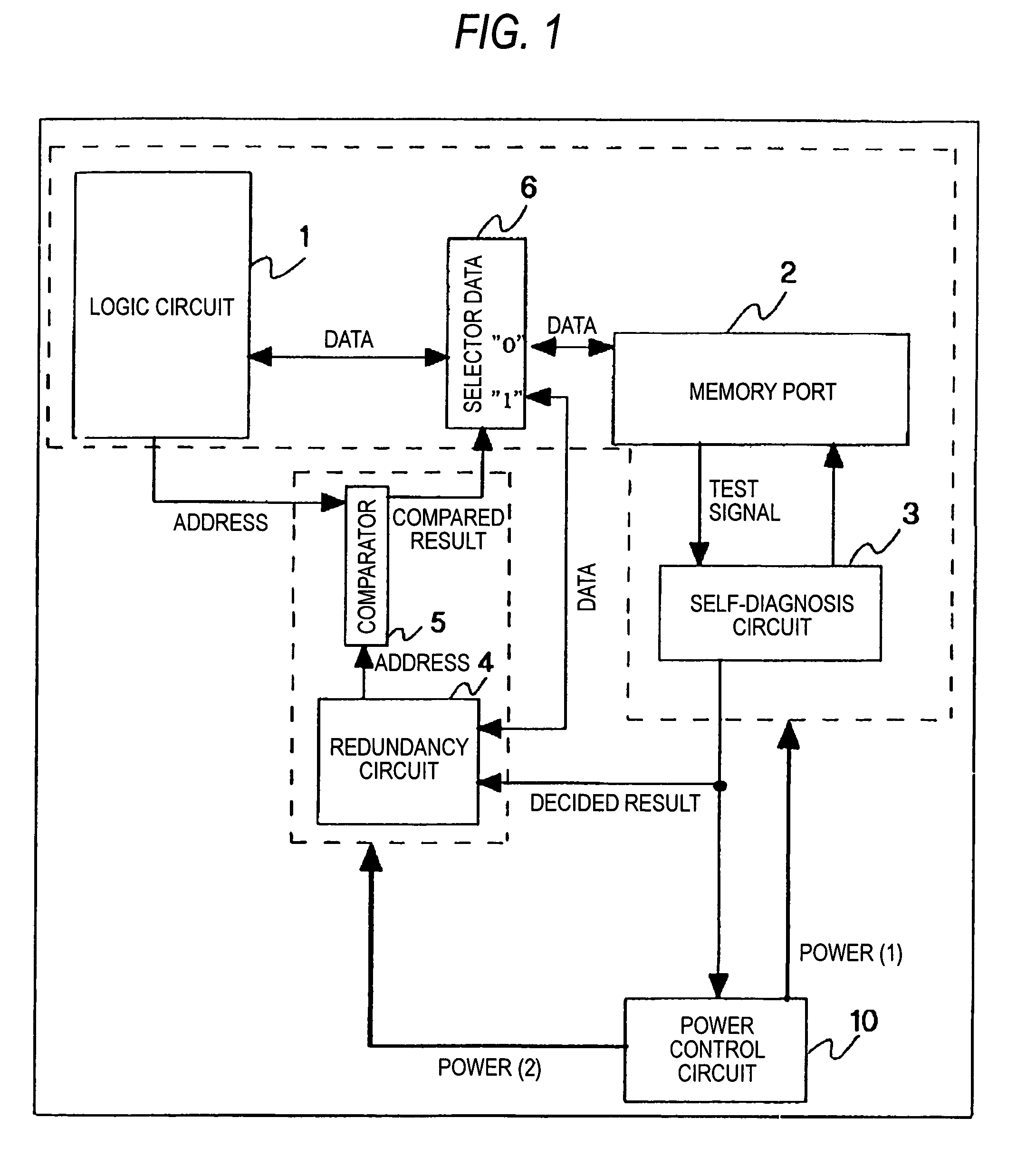
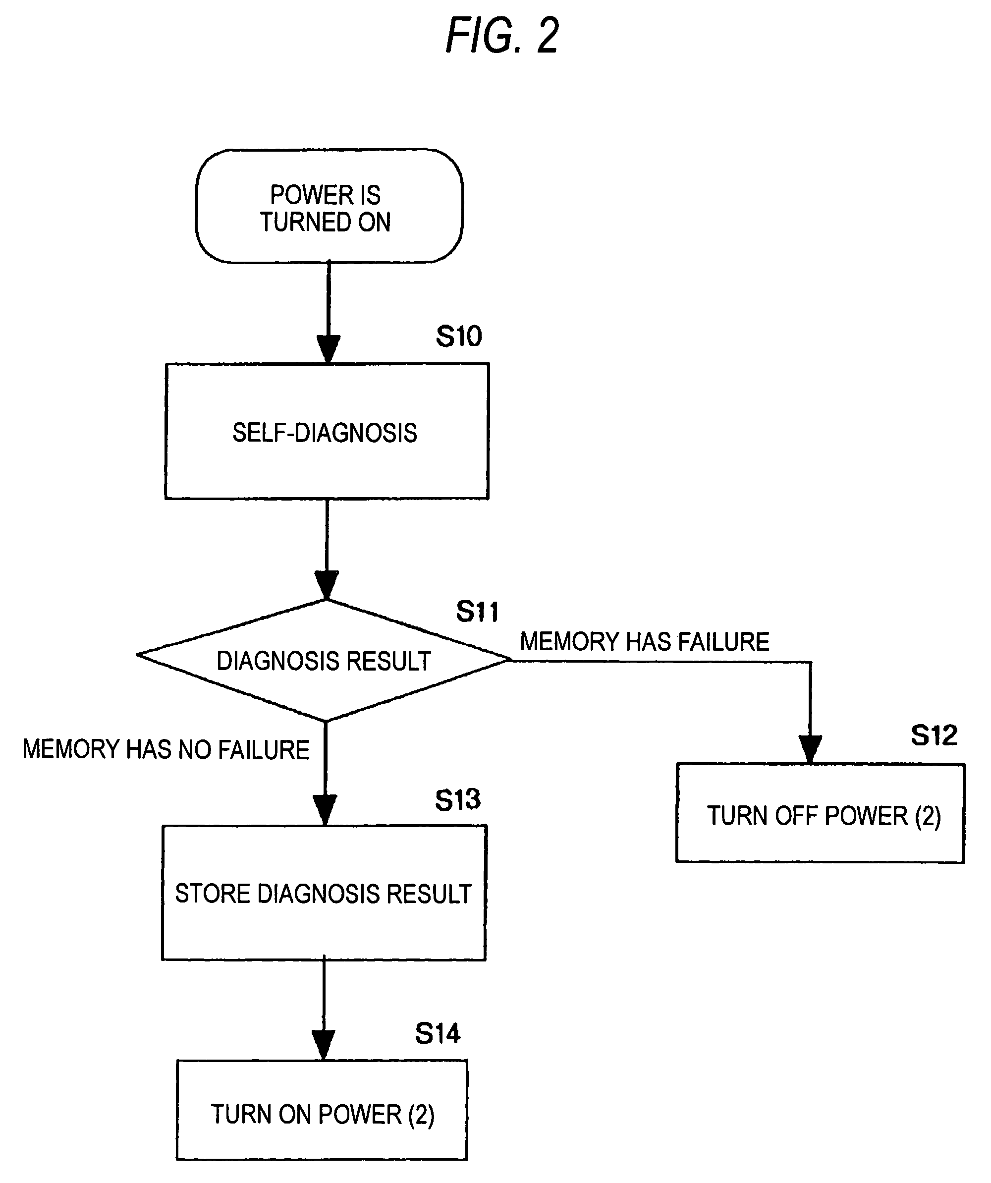
[0018]FIG. 1 is a diagram showing the structure of a memory trouble relief device according to the first embodiment of the present invention.

[0019]The memory trouble relief device comprises a logic circuit 1 for realizing an actual function, a memory part 2 used by the logic circuit 1, a self-diagnosis circuit 3 for recognizing whether or not the failure of the memory part 2 is present, a redundancy circuit 4 for performing a replacement of the defective part of the memory part 2 by control of fuse or the like, on the basis of the decided result of the self-diagnosis circuit 3, a comparator 5 for comparing the address of the memory designated by the logic circuit 1 with determination result (address which indicates the failure part) outputted from the redundancy circuit 3 and a selector 6 for selectively allowing the logic circuit 1 to access the redundancy relief circuit 4 when the memory is failed in accordance with the result of the comparator 5.

[0020]Power (1) ...

second embodiment

(Second Embodiment)

[0023]FIG. 3 is a block diagram showing the structure of a memory trouble relief circuit according to the second embodiment of the invention. The description will be made with like reference numerals given to the same parts as in FIG. 1. In FIG. 3, the memory trouble relief circuit comprises a logic circuit 1, a memory part 2, a redundancy circuit 4, a Flash memory 9 for holding the inspected result of a semiconductor integrated circuit, a comparator 5 for comparing an address designated by the logic circuit 1 with a decided result stored in the Flash memory 9, a selector 6 for enabling the logic circuit 1 to access the redundancy circuit 4 when the compared result of the comparator 5 indicates that the memory part 2 has a defective memory cell.

[0024]Power (1) is supplied to the semiconductor integrated circuit having the logic circuit 1, memory part 2 and selector 6. Power (2) is supplied to a redundancy relief circuit having the redundancy circuit 4 and comparat...


PUM


Abstract

When a redundancy circuit is provided to relieve the inferiority of a semiconductor storage device, and then, the semiconductor storage device has no defect, power is inconveniently supplied even to the unused redundancy circuit to generate unnecessary leakage current.A self-diagnosis circuit for a semiconductor storage device is provided to perform the self-diagnosis of the semiconductor storage device upon turning on a power source. Power (2) is supplied to a redundancy circuit part and power (1) is supplied to a circuit part except the redundancy circuit part. When the semiconductor storage device has no defect as a result of the self-diagnosis, a control for turning off the power (2) of the redundancy circuit part is performed.

Description

BACKGROUND OF THE INVENTION[0001]1. Field of the Invention[0002]The present invention relates to a semiconductor storage device for performing a redundancy relief in the semiconductor storage device.[0003]2. Description of the Related Art[0004]With the progress of miniaturization of a semiconductor, the semiconductor including a semiconductor storage device has usually had a redundancy circuit to relieve the defect of a semiconductor device part. When a defect is detected in the storage device part upon inspection, the storage device part has been replaced by the redundancy circuit part to realize the improvement of a yield of the semiconductor. (JP-A-11-238393 or the like)[0005]However, in the usual semiconductor including the semiconductor storage device, when the defect is not detected in the semiconductor storage device part upon inspection, a redundancy relief circuit is not used, so that leakage current is inconveniently generated even in the unused circuit.SUMMARY OF THE INVE...

Claims


Application Information

Patent Timeline
Patent Type & Authority Patents(United States)
IPC IPC(8): G06F11/00G11C11/40G11C7/00G11C11/00G11C7/24G11C11/4063G11C29/00H01L21/70H01L21/822H01L21/82H01L27/10H01L27/04G11C29/02G11C29/04
CPCG11C29/83G11C2029/0407
Inventor MIZUKOSHI, NORIKO
Owner PANASONIC CORP
Why Eureka
Try Eureka