Master-slave-type scanning flip-flop circuit for high-speed operation with reduced load capacity of clock controller

a flip-flop circuit and clock controller technology, applied in pulse generators, instruments, pulse techniques, etc., can solve the problems of increased delay time and inability to test, and achieve the effect of suppressing an increase in delay time and speed

Inactive Publication Date: 2005-11-22
NEC CORP
View PDF5 Cites 34 Cited by
  • Summary
  • Abstract
  • Description
  • Claims
  • Application Information

AI Technical Summary

Benefits of technology

[0057]It is therefore an object of the present invention to provide a scanning flip-flop circuit which is capable of operating at a higher speed while suppressing an increase in a delay time that is caused by adding a testing circuit.
[0059]In the above scanning flip-flop circuit, since the second scan controller is connected to the output terminal of the first scan controller, rather than the clock controller, the load capacity of the clock controller connected in a signal path when the scanning flip-flop circuit is in the normal mode of operation is reduced to shorten a delay time.
[0062]In the above scanning flip-flop circuits, since the scan controller is connected to the output terminal of the master latch, rather than the clock controller, the load capacity of the clock controller connected in a signal path when the scanning flip-flop circuit is in the normal mode of operation is reduced to shorten a delay time. therefore, the overall delay time of the scanning flip-flop circuit is shortened. The scanning flip-flop circuits according to the present invention can use many resources of conventional flip-flop circuits because they do not need changes in logic operation.

Problems solved by technology

Since semiconductor integrated circuit devices (hereinafter referred to as “LSI circuits”) in recent years are larger in scale and more highly packed than before, it is impossible to test them unless their LSI chips incorporate some design for making the test easier.
With the conventional scanning flip-flop circuit shown in FIG. 1, since not only inverter INV21 and transfer gate TG21 of slave latch 2 used in the normal mode of operation, but also transfer gate TG71 of scan controller 7 used in the scan mode of operation are connected as loads to the output terminal of transfer gate TG61 of clock controller 6 which is connected in a signal path for the normal mode of operation, the load capacity of transfer gate TG61 is increased, resulting in an increase in the delay time.

Method used


Image

  • Master-slave-type scanning flip-flop circuit for high-speed operation with reduced load capacity of clock controller
  • Master-slave-type scanning flip-flop circuit for high-speed operation with reduced load capacity of clock controller
  • Master-slave-type scanning flip-flop circuit for high-speed operation with reduced load capacity of clock controller

Examples


Embodiment Construction

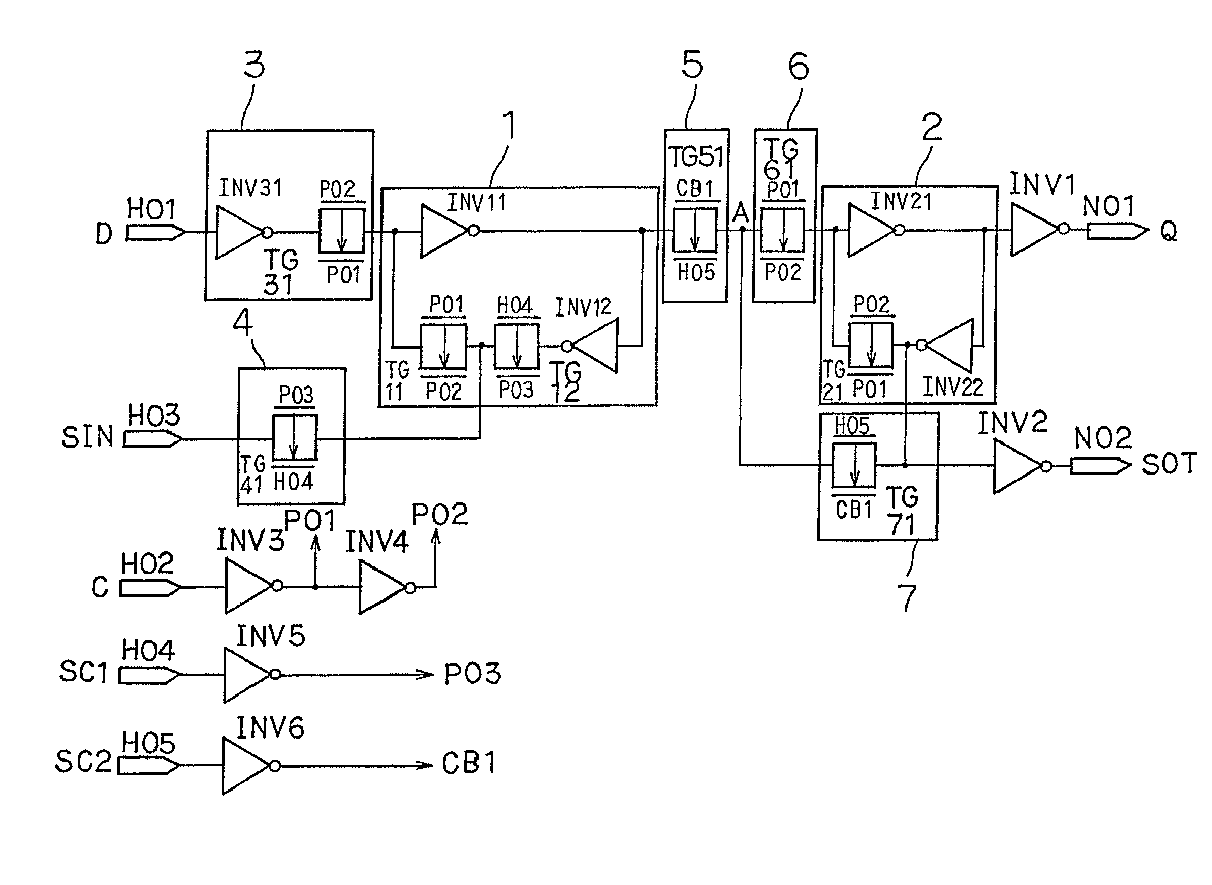
[0071]As shown in FIG. 5, a scanning flip-flop circuit according to an embodiment of the present invention comprises master latch 1, slave latch 2, clock controller 3, scan controller 4, scan controller 5, clock controller 6, and scan controller 7.

[0072]Master latch 1 temporarily holds data signal D or scan-in signal SIN. Slave latch 2 temporarily holds an output signal from master latch 1 in synchronism with clock C for normal operation. Clock controller 3 outputs data signal D to master latch 1 in synchronism with clock C. Scan controller 4 outputs scan-in signal SIN to master latch 1 in synchronism with scan clock SC1. Scan controller 5 receives the output signal from master latch 1 and outputs the received signal in synchronism with scan clock SC2. Clock controller 6 receives the output signal from the scan controller 5 and outputs the received signal to slave latch 2 in synchronism with clock C. Scan controller 7 outputs scan-out signal SOT which represents a scan result in syn...


PUM


Abstract

A master-slave-type scanning flip-flop circuit is capable of operating at a higher speed by reducing a load capacity of a clock controller. The master-slave-type scanning flip-flop circuit is used to test a semiconductor integrated circuit device, and has a master latch and a slave latch each for temporarily holding an input signal, a first scan controller, a clock controller, and a second scan controller. The first scan controller receives an output signal from the master latch and outputs the received output signal in synchronism with a scan clock which is a clock for testing the semiconductor integrated circuit device, when the semiconductor integrated circuit device is tested. The clock controller receives an output signal from the first scan controller and outputs the received output signal to the slave unit in synchronism with a predetermined clock when in a normal mode of operation. The second scan controller has an input terminal connected to an output terminal of the first scan controller, and outputs a scan-out signal corresponding to a scan-in signal which is an input signal for testing the semiconductor integrated circuit device, in synchronism with the scan clock when the semiconductor integrated circuit device is tested.

Description

BACKGROUND OF THE INVENTION[0001]1. Field of the Invention[0002]The present invention relates to a scanning flip-flop circuit for use as a flip-flop circuit in testing a semiconductor integrated circuit device.[0003]2. Description of the Related Art[0004]Since semiconductor integrated circuit devices (hereinafter referred to as “LSI circuits”) in recent years are larger in scale and more highly packed than before, it is impossible to test them unless their LSI chips incorporate some design for making the test easier. One known method of making LSI circuit tests easier is a scan path method. According to the scan path method, various flip-flop circuits in an LSI circuit are connected in a chain pattern so as to operate as a shift register, and, when the LSI circuit is tested, the shifting function of the shift register is used to control and observe values of the flip-flop circuits from outside of the LSI circuit.[0005]In order to test an LSI circuit according to the scan path method...

Claims


Application Information

Patent Timeline
Patent Type & Authority Patents(United States)
IPC IPC(8): G01R31/3185G01R31/28H03K3/037H03K3/3562H03K19/00
CPCG01R31/318525G01R31/318541G01R31/318555
Inventor MATSUSHIMA, YUSUKE
Owner NEC CORP
Why Eureka
Try Eureka