Method of manufacturing liquid crystal display device

a liquid crystal display and manufacturing method technology, applied in non-linear optics, instruments, optics, etc., can solve the problems of preventing the occurrence of distortion of substrates in the vicinity of main seal patterns, and achieve the effects of preventing distortion, excellent display quality, and high yield

Inactive Publication Date: 2005-11-29
SHARP KK
View PDF6 Cites 52 Cited by
  • Summary
  • Abstract
  • Description
  • Claims
  • Application Information

AI Technical Summary

Benefits of technology

[0020]Based on the above description, an object of the present invention is to provide a method of manufacturing a liquid crystal display device whereby substrates are prevented from distorting when a pair of substrates is bonded with a sealant, and liquid crystal display devices with excellent display quality can be manufactured with high yield.
[0022]For example, in the case where dummy patterns are constituted of a plurality of first dummy seal patterns which respectively enclose each of a plurality of main seal patterns, and one second dummy seal pattern which encloses all the plurality of first dummy seal patterns, vacuum is maintained inside the first dummy seal patterns enclosing the main seal patterns even though faulty adhesion occurs either in the sealant which constitutes the first dummy seal patterns or in the sealant which constitutes the second dummy seal pattern. This enables pressure to be applied to the entire inside of the first dummy seal patterns in a perpendicular direction with respect to a substrate when the pair of the substrates is exposed to atmospheric pressure again. Consequently, occurrence of distortion of substrates in the vicinity of the main seal patterns is impeded. As a result, faulty display due to distortion of the substrates is prevented, and manufacturing yield of liquid crystal display devices will improve.
[0023]In addition, for example, dummy seal patterns are constituted of a plurality of first dummy seal patterns and a plurality of second dummy seal patterns. The plurality of first dummy seal patterns respectively enclose individual main seal patterns, and the plurality of second dummy seal pattern interconnect between sides of the first dummy seal pattern facing sides of one substrate. Thereupon, when the inside of the chamber of the assembling device is recovered to atmospheric pressure, vacuum is maintained in the central portions of the substrates by the second dummy seal patterns. This also applies pressure to the central portions of the substrates in a vertical direction with respective to the substrates, and adhesion is improved between the substrates and the sealant which constitutes the first dummy seal patterns. As a result, faulty display due to distortion of the substrates is prevented, and thus manufacturing yield of liquid crystal displays is improved.

Problems solved by technology

Consequently, occurrence of distortion of substrates in the vicinity of the main seal patterns is impeded.

Method used


Image

  • Method of manufacturing liquid crystal display device
  • Method of manufacturing liquid crystal display device
  • Method of manufacturing liquid crystal display device

Examples


first embodiment

(First Embodiment)

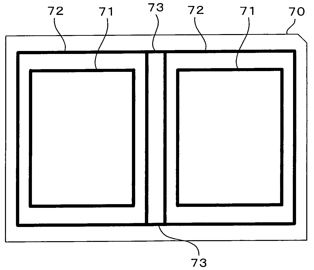
[0044]FIGS. 7A to 7G are diagrams illustrating a method of manufacturing liquid crystal displays in a first embodiment of the present invention. Herein, a case where two liquid crystal displays are simultaneously manufactured by use of mother glass substrates, known as a two-panels-per-sheet output, is described.

[0045]First, two mother glass substrates are prepared. As shown in FIGS. 7A and 7B, gate bus lines 11a, data bus lines 13, TFTs 14, pixel electrodes 16, alignment films 17 and the like are respectively formed in the right and left half areas in one of the mother glass substrates, which is to be a TFT substrate. In addition, color filters 22, common electrodes 23, protrusions 24, alignment films 25, columnar spacers 26 and the like are respectively formed in the right and left half areas in the other mother glass substrate, which is to be a CF substrate.

[0046]Subsequently, as shown in FIG. 7A, main seal patterns 51 which individually enclose each display are...

second embodiment

(Second Embodiment)

[0067]FIGS. 9A and 9B are diagrams illustrating a method of manufacturing a liquid crystal display device in a second embodiment of the present invention. Herein, a case of a two-panels-per-sheet output is described where two liquid crystal display devices are simultaneously formed by use of mother glass substrates. Note that the present embodiment is also described with reference to FIGS. 5 and 6.

[0068]First, two mother glass substrates are prepared. As shown in FIGS. 5 and 6, gate bus lines 11a, data bus lines 13, TFTs 14, pixel electrodes 16, alignment films 17 and the like are respectively formed in the right and left half areas in one of the mother glass substrates, which is to be a TFT substrate. In addition, color filters 22, common electrodes 23, protrusions 24, alignment films 25, columnar spacers 26 and the like are respectively formed in the right and left half areas in the other mother glass substrate, which is to be a CF substrate.

[0069]Second, as sho...


PUM

PropertyMeasurementUnit
heightsaaaaaaaaaa
heightsaaaaaaaaaa
pressureaaaaaaaaaa

Abstract

A plurality of main seal patterns and dummy seal patterns are formed by a sealant on one of substrates. The plurality of main seal patterns individually enclose each of a plurality of display areas. The dummy seal patterns individually enclose the plurality of main seal patterns, and sides of the dummy seal patterns facing sides of the one substrate are all interconnected. These formations enable constant vacuum levels to be maintained the inside and the outside of the main seal patterns when the inside of a chamber of an assembling device is recovered to atmospheric pressure. Therefore, distortion of substrates is impeded in the vicinity of the main seal patterns, and degradation of display quality can be prevented.

Description

CROSS-REFERENCE TO RELATED APPLICATIONS[0001]This application is based upon and claims priority of Japanese Patent Application No. 2002-253135, filed on Aug. 30, 2002, the contents being incorporated herein by reference.BACKGROUND OF THE INVENTION[0002]1. Field of the Invention[0003]The present invention relates to a method of manufacturing a liquid crystal display device by a one-drop-fill process, and more particularly to a method of manufacturing liquid crystal displays whereby the plurality of liquid crystal display devices are simultaneously formed by use of large substrates.[0004]2. Description of the Prior Art[0005]Liquid crystal display devices have been widely used for various kinds of electronic equipment since liquid crystal displays are thin and light and have merits of being driven with low voltage and consuming less electric power.[0006]Common liquid crystal displays used for televisions and personal computers are constituted such that liquid crystals are enclosed betw...

Claims


Application Information

Patent Timeline
Patent Type & Authority Patents(United States)
IPC IPC(8): G02F1/13G02F1/1339G02F1/1341
CPCG02F1/1339G02F1/1341G02F2001/13415G02F1/13415
Inventor KIDA, TETSUYAMURATA, SATOSHI
Owner SHARP KK
Why Eureka
Try Eureka