
Display device and driving method of the same

a technology of display devices and driving methods, applied in static indicating devices, instruments, optics, etc., can solve the problems of inability to completely correct the above defects, inability to determine whether, and easily occur defects during the manufacturing process, so as to improve productivity, reduce the cost of display devices, and increase the yield of display devices

Inactive Publication Date: 2005-11-29
SHARP KK
View PDF10 Cites 20 Cited by
  • Summary
  • Abstract
  • Description
  • Claims
  • Application Information

AI Technical Summary

Benefits of technology

[0029]It is another object of the present invention to provide a display device capable of reliably detecting a defect with which the potential of an output line of a scanning driver is fixed or unfixed, and a driving method of the device.
[0030]It is still another object of the present invention to provide a display device capable of reliably correcting a defect with which the potential of an output line of a scanning driver is fixed or unfixed, and a driving method of the device.
[0033]Even when the scanning driver has a defect or the scanning driver and display section have defects, the defect can be automatically corrected, so normal display can be performed. In addition, since the automatic correction of the display device is possible, the yield of display devices can be increased, the productivity can be improved, and the cost of display devices can be reduced.

Problems solved by technology

As a consequence, defects during the manufacturing process readily occur in the scanning drivers 101a and 101b at high probability.
Additionally, even if the defect in the second line can be visually detected on the display screen, it cannot be determined whether the defect in the second line is due to a short circuit in the scanning driver 101a or in the scanning driver 101b.
The above defects cannot be completely corrected.
However, the third prior art discloses only the check method and no correction method.
The correction method has limitations and cannot correct the defects shown in FIGS. 25 and 26.
Details of the check method are not presented, and all defects cannot always be detected.

Method used


Image

  • Display device and driving method of the same
  • Display device and driving method of the same
  • Display device and driving method of the same

Examples


first embodiment

(First Embodiment)

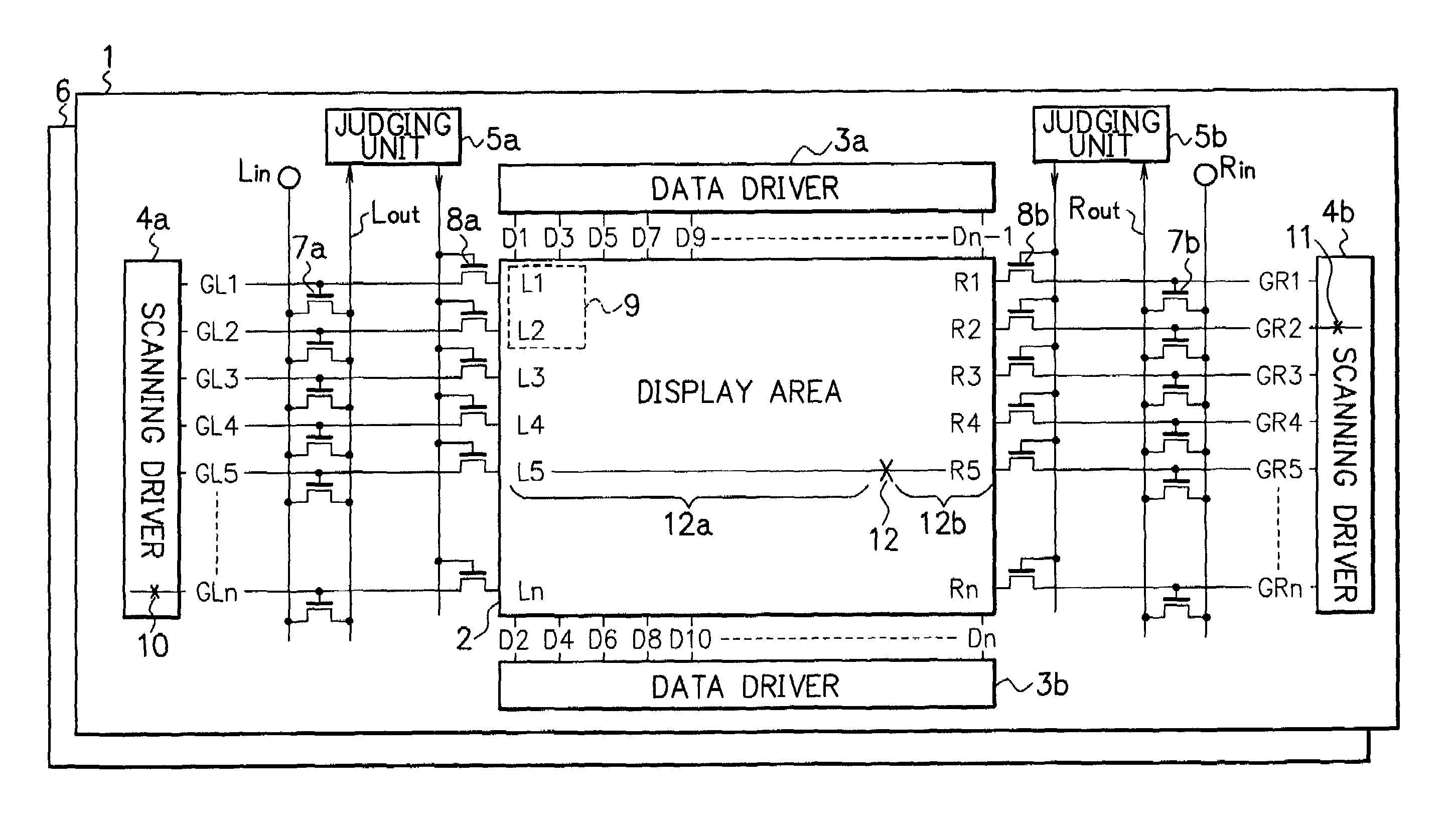
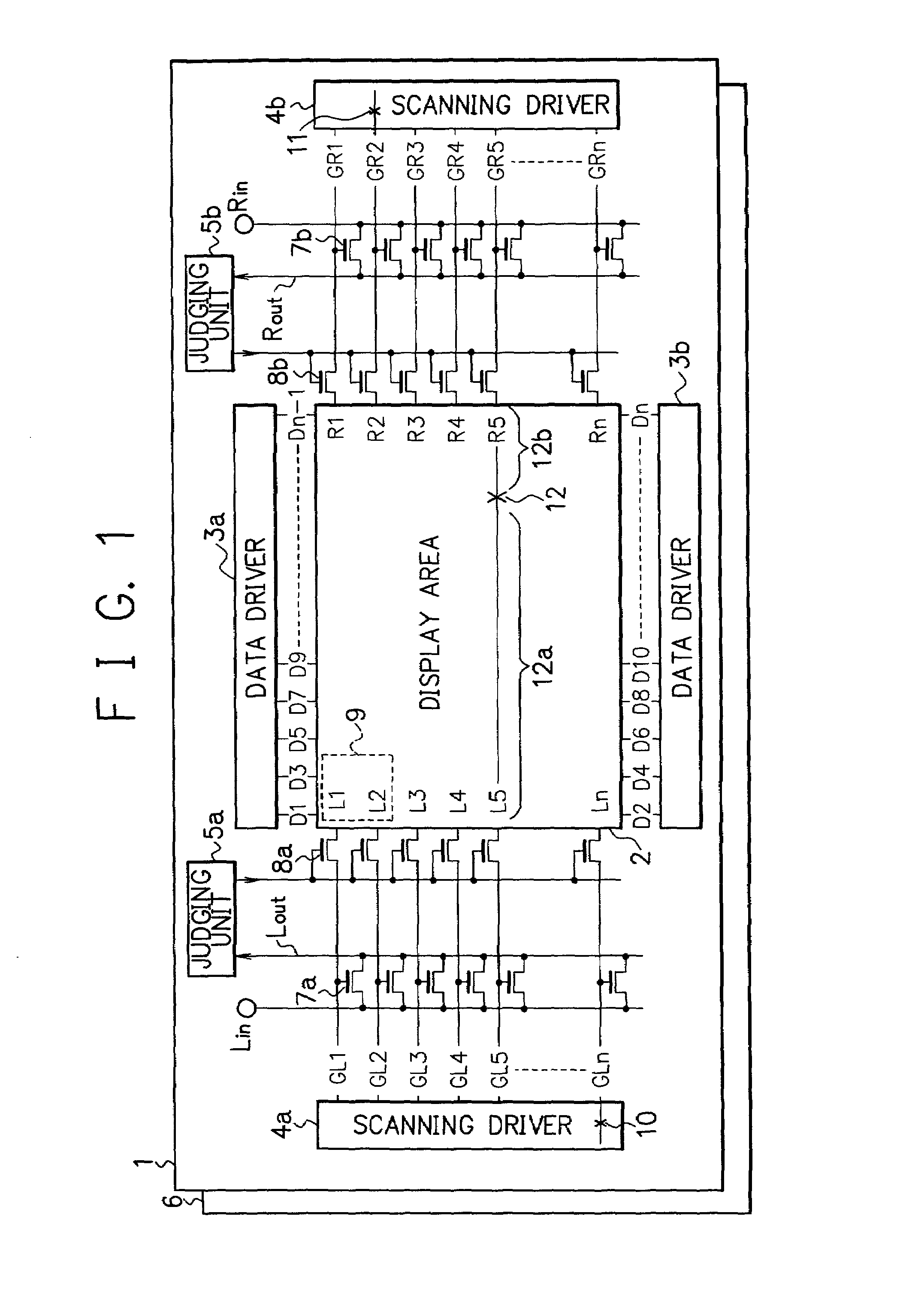
[0064]FIG. 1 is a block diagram showing the structure of a liquid crystal display device according to the first embodiment of the present invention. When an output line in a first or second scanning driver 4a or 4b has a short circuit to the ground line or disconnection and is fixed at low level or unfixed, the liquid crystal display device according to the first embodiment can detect the defect and automatically correct it.

[0065]In addition to a display area 2, a first scanning driver 4a, a second scanning driver 4b, a first data driver 3a, and a second data driver 3b, judging units 5a and 5b and n-channel MOS transistors 7a, 7b, 8a, and 8b are integrally formed on a glass substrate 1. The space between the glass substrate 1 and a counter substrate 6 is filled with liquid crystal. Counter electrodes are formed on the entire surface of the counter substrate 6. The second to fifth embodiments to be described later also use similar counter substrates 6. All transisto...

second embodiment

(Second Embodiment)

[0111]FIG. 8 is a block diagram showing the structure of a liquid crystal display device according to the second embodiment of the present invention. The second embodiment is different from the first embodiment only in that n-channel MOS transistors 14a and 14b, p-channel MOS transistors 15a and 15b, and inverters 13a and 13b are provided in place of the switching transistors 8a and 8b in the first embodiment.

[0112]The portion on a first scanning driver 4a side will be described first. A CMOS (Complementary MOS) transistor made up from an n-channel MOS transistor 14a and a p-channel MOS transistor 15b forms a switch. One of the source and drain of each of the transistors 14a and 15a is connected to output lines GL1 to GLn of the first scanning driver 4a, and the other is connected to scanning lines L1 to Ln in a display area 2. The gates of n-channel MOS transistors 14a are connected to the output of a judging unit 5a. A signal obtained by logically inverting the ...

third embodiment

(Third Embodiment)

[0115]FIG. 9 is a block diagram showing the structure of a liquid crystal display device according to the third embodiment of the present invention. In the third embodiment, the output lines in first and second scanning drivers 71a and 71b are short-circuited to power supply line, so when a defect to fix an output line at high level is generated, the defect can be detected and automatically corrected.

[0116]In addition to a display area 2, a first data driver 3a, a second data driver 3b, a first scanning driver 71a, and a second scanning driver 71b, judging units 72a and 72b, NAND circuits 73a and 73b, inverters 74a, 74b, 76a, and 76b, n-channel MOS transistors 75a, 75b, 77a, and 77b, and p-channel MOS transistors 78a and 78b are integrally formed on a glass substrate 1.

[0117]The display area 2 and the first and second data drivers 3a and 3b are the same as in the first embodiment (FIG. 1). The first scanning driver 71a additionally has a 0th output line GL0 and (n+...


PUM

PropertyMeasurementUnit
power supply potentialaaaaaaaaaa
temperatureaaaaaaaaaa
areaaaaaaaaaaa

Abstract

A display device has a display section having scanning lines, and first and second scanning drivers having output lines for supplying scanning signals to the two ends of the scanning lines in the display section. When the potential of at least one of the output lines of the first or second scanning driver is fixed or unfixed due to an error in the first or second scanning driver, the output line at the fixed or unfixed potential is disconnected from the corresponding scanning line in the display section.

Description

CROSS-REFERENCE TO RELATED APPLICATIONS[0001]This application is based upon and claims priority of Japanese Patent Applications No. 2000-211661, filed on Jul. 12, 2000, the contents being incorporated herein by reference.BACKGROUND OF THE INVENTION[0002]1. Field of the Invention[0003]The present invention relates to display devices and driving methods of the devices, particularly to display devices that make a display in accordance with a scanning signal supplied from a scanning driver, and driving methods of the devices.[0004]2. Description of the Related Art[0005]In recent research and development of liquid crystal display devices, keen competition is held for technologies for cost reduction. In particular, a technique of forming a polysilicon thin-film transistor by a low-temperature process makes it possible to form not only a display area but also a peripheral circuit (e.g., a driver) on an inexpensive glass substrate. This technique has received a great deal of attention becau...

Claims


Application Information

Patent Timeline
Patent Type & Authority Patents(United States)
IPC IPC(8): G01R31/02G02F1/133G09G3/20G09G3/36
CPCG09G3/3648G09G3/3677G09G3/3688G09G2300/0408G09G2310/0281G09G2310/0297G09G2330/08G09G2330/12G09G2352/00G02F1/133
Inventor MORITA, KEIZONAKABAYASHI, KEN-ICHI
Owner SHARP KK
Learn More