Pixel defect correction device

a defect correction and pixel technology, applied in the field of pixel defect correction devices, can solve the problems of reducing the size of the photodiode and the v transfer path increasing the probability of defect generation, white flaw, and black flaw

Inactive Publication Date: 2009-09-22
MONUMENT PEAK VENTURES LLC
View PDF4 Cites 11 Cited by
  • Summary
  • Abstract
  • Description
  • Claims
  • Application Information

AI Technical Summary

Benefits of technology

[0038]The present invention was conceived in view of the above-described circumstances and advantageously provides a device which can simultaneously correct a point flaw and a vertical flaw; a point flaw and a horizontal flaw; or a point flaw, a vertical flaw, and a horizontal flaw.
[0043]Through use of the present invention, a point defect pixel and a line defect pixel can be reliably corrected, and a point defect pixel and a line defect pixel can be corrected simultaneously and in parallel to each other.

Problems solved by technology

While the reduction of the pixel size can be achieved by reducing the size of the photodiode and vertical direction (V) transfer path, reduction of the size of the photodiode and the V transfer path increases the probability of generation of defects.
A localized crystal defect of a photodiode causes pixel degradation and defects in which a constant bias voltage is always applied to an opto-electric conversion output corresponding to an amount of incident light causes a white spot with a high brightness on the monitor, and thus causes a defect which is commonly called a white flaw.
A defect in which the photosensitivity of the photodiode is reduced appears on the monitor as a black point, and thus causes a defect which is commonly called a black flaw.
A defect in which a dust or like is attached to the V transfer path blocks transfer of charges and appears on the monitor as a linear flaw, and thus causes a defect which is commonly called a vertical flaw.
When the point flaw and the vertical flaw are sequentially corrected as described above, correction circuits for both processes are required, and, moreover, the correction process requires a long time before all defects are corrected.
When, however, the point flaw and the vertical flaw are simultaneously processed in the related art as described above, there is a problem in that the precision of the correction is degraded when the point flaw and the vertical flaw are present adjacent to each other.
The above-described problem may occur not only when the point flaw and the vertical flaw are simultaneously corrected, but also when the G pixel, R pixel, and B pixel are simultaneously corrected and when the vertical flaw and a horizontal flaw are simultaneously corrected in a case in which the horizontal flaw and vertical flaw may simultaneously occur because of a gate switch defect of a CMOS.

Method used


Image

  • Pixel defect correction device
  • Pixel defect correction device
  • Pixel defect correction device

Examples


Embodiment Construction

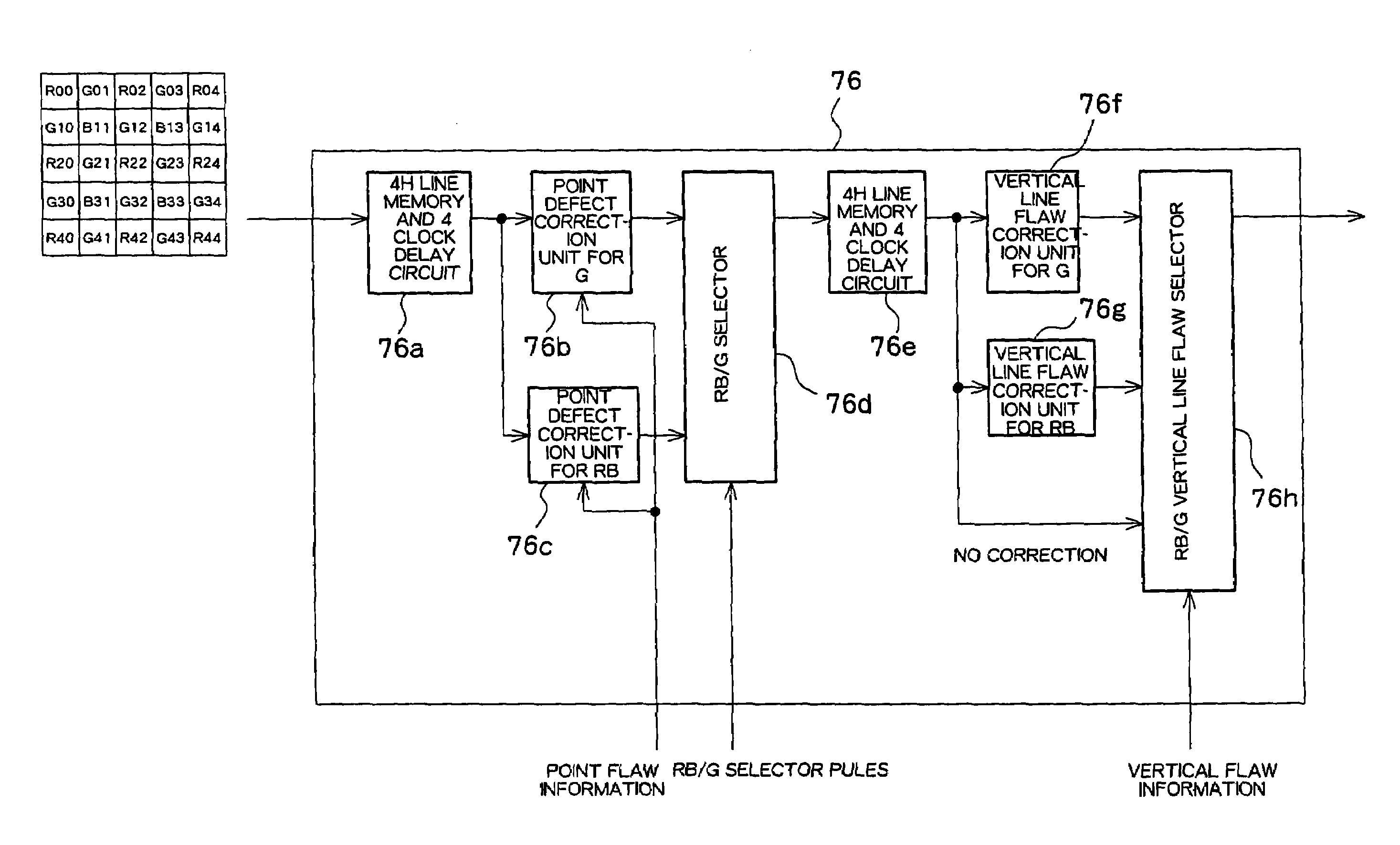
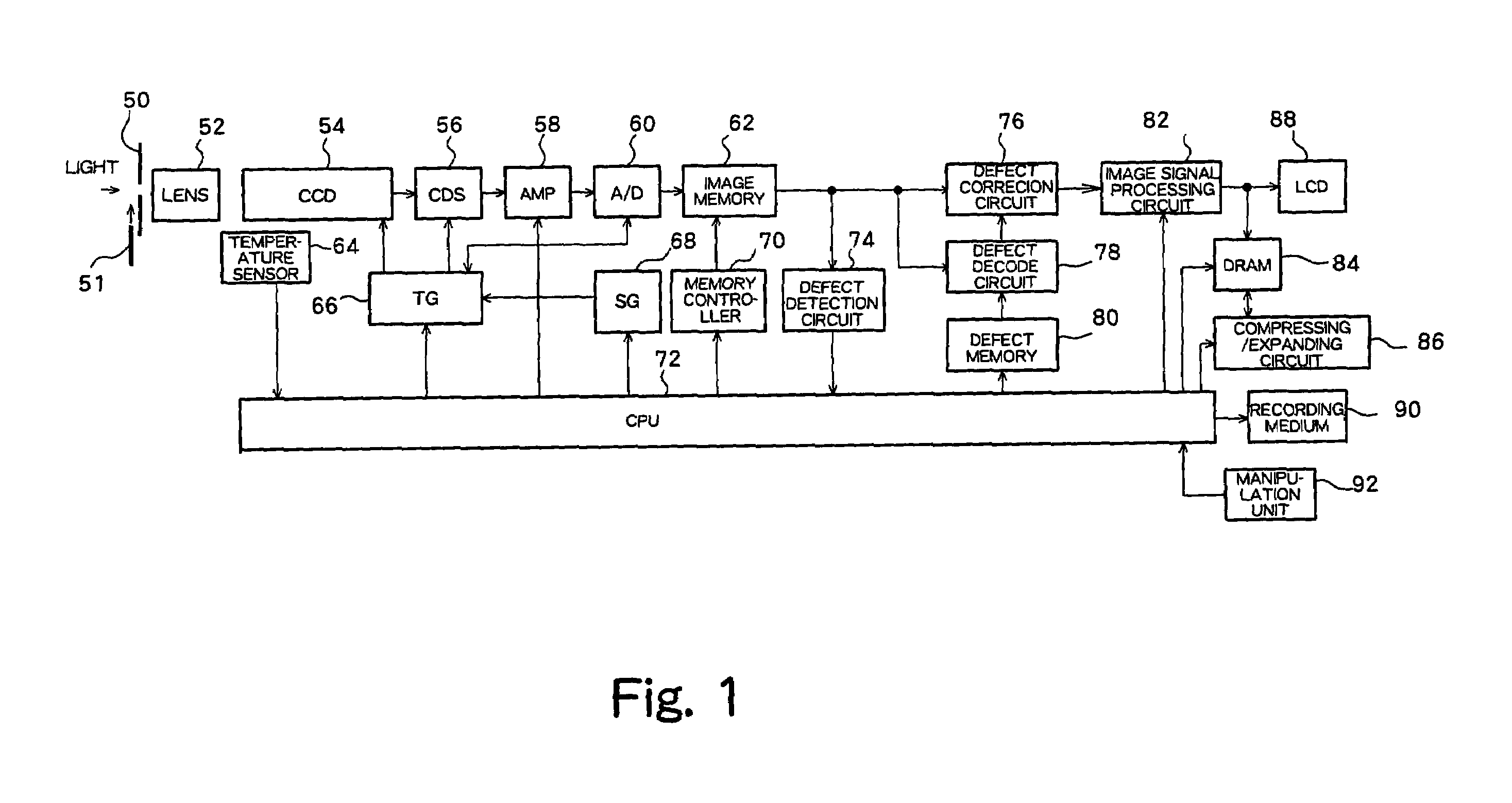
[0104]Preferred embodiments of the present invention will now be described referring to the drawings. FIG. 1 shows an overall structure of a digital camera incorporating a pixel defect correction circuit according to a first preferred embodiment of the present invention. An optical system including a diaphragm 50 and a lens 52 guides light from an imaging target to a CCD 54. A light shielding filter 51 may be placed in front of the diaphragm 50. The CCD 54 converts the light from the imaging target into an electrical signal corresponding to the amount of light and supplies the electrical signal to a CDS (correlated double sampling) 56. The CDS 56 samples the image signal and supplied to an A / D 60 through an amplifier (AMP) 58. The amplifier (AMP) 58 adjusts a gain of the image signal. The A / D 60 converts the sampled image signal into a digital signal and supplies the digital signal to an image memory 62 which functions as a frame memory. Operations of the CCD 54, CDS 56, and A / D 60 ...


PUM


Abstract

A point defect and a line defect in a captured image resulting due to an imaging element defect in a digital camera are interpolated. A defect correction circuit of a digital camera simultaneously corrects a point flaw, a vertical line flaw, and a horizontal line flaw in a captured image. In consideration of cases in which a point flaw and a vertical line flaw are present adjacent to each other, the defect correction circuit executes predetermined difference calculations using pixels surrounding a target pixel to be corrected and determines an interpolation pattern based on a comparison of magnitude among the difference calculation values. The defect correction circuit also selects, for interpolation, an interpolation pattern from among interpolation patterns prepared in advance based on an adjacent pattern of the point flaw and line flaw. The adjacent pattern is detected by a defect decode circuit 78.

Description

FIELD OF THE INVENTION[0001]The present invention relates to a pixel defect correction device, and in particular to a technique for correcting point defects, horizontal direction defects, and vertical direction defects in two-dimensional pixels arranged along horizontal and vertical directions.BACKGROUND OF THE INVENTION[0002]CCD's and CMOS's are used as imaging elements in digital cameras. In order to respond to a demand for higher image quality, efforts have been made to reduce pixel size and increase the number of pixels. While the reduction of the pixel size can be achieved by reducing the size of the photodiode and vertical direction (V) transfer path, reduction of the size of the photodiode and the V transfer path increases the probability of generation of defects. A localized crystal defect of a photodiode causes pixel degradation and defects in which a constant bias voltage is always applied to an opto-electric conversion output corresponding to an amount of incident light c...

Claims


Application Information

Patent Timeline
Patent Type & Authority Patents(United States)
IPC IPC(8): G06K9/00H04N5/335H04N5/367H04N5/372
CPCH04N5/367H04N25/68
Inventor SAKURAI, JUNZO
Owner MONUMENT PEAK VENTURES LLC
Why Eureka
Try Eureka