Liquid crystal display device having a noise shielding member

Active Publication Date: 2005-12-06
SAMSUNG DISPLAY CO LTD
View PDF7 Cites 26 Cited by
  • Summary
  • Abstract
  • Description
  • Claims
  • Application Information

AI Technical Summary

Benefits of technology

[0025]According to the above exemplary embodiments, the noise shielding means comprised of conductive material is formed between the light source and the liquid crystal display panel. Accordingly, the displ

Problems solved by technology

However, the LCD devices have the following problems due to the backlight assembly.
The electromagnetic waves due to the high voltage signal applied to the lamps cause electromagnetic disturbance in the liquid crystal display panel and changes the electromagnetic characteristics of the liquid crystal display panel, so that display failure

Method used


Image

  • Liquid crystal display device having a noise shielding member
  • Liquid crystal display device having a noise shielding member
  • Liquid crystal display device having a noise shielding member

Examples


first modified embodiment

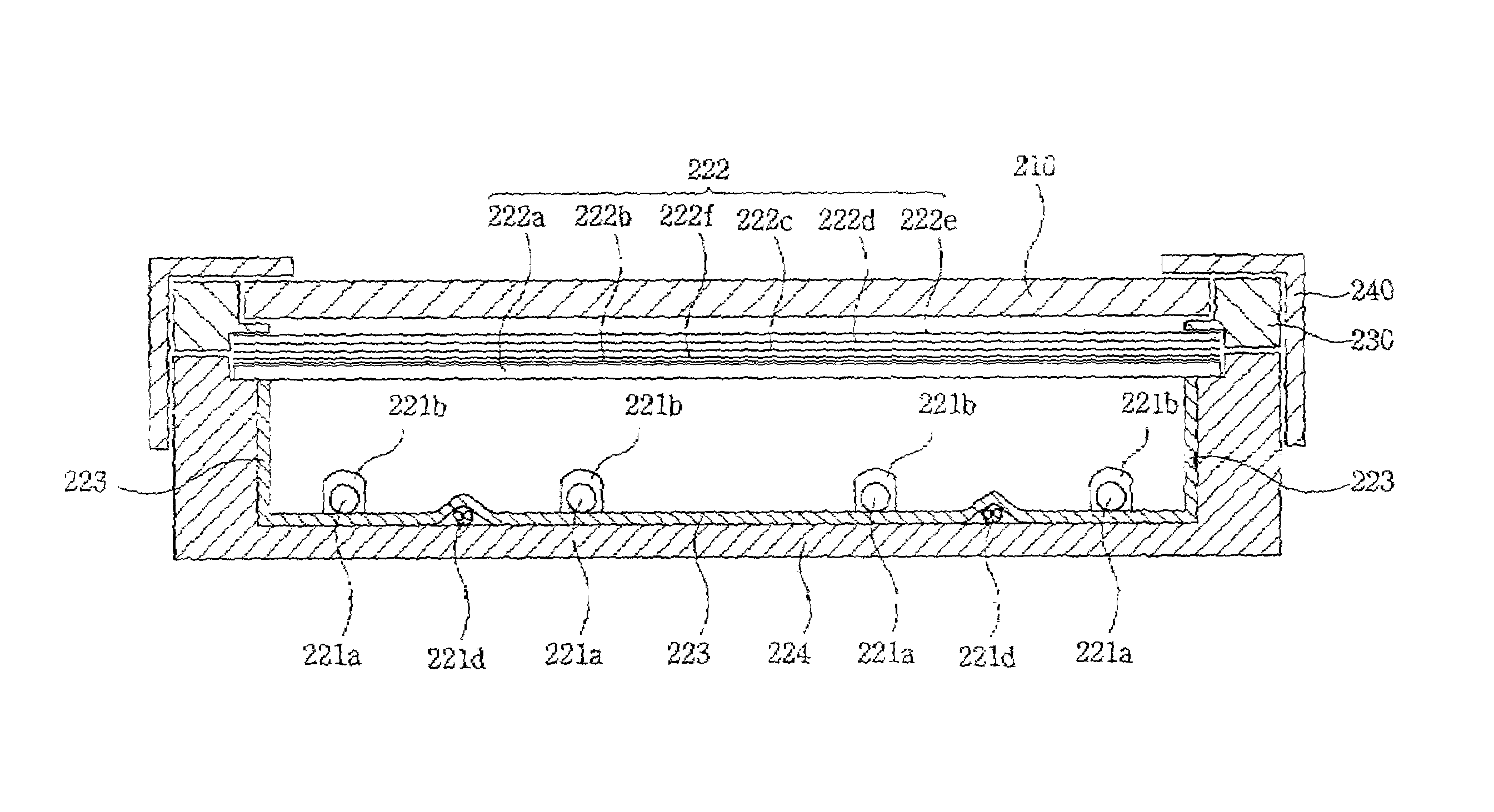
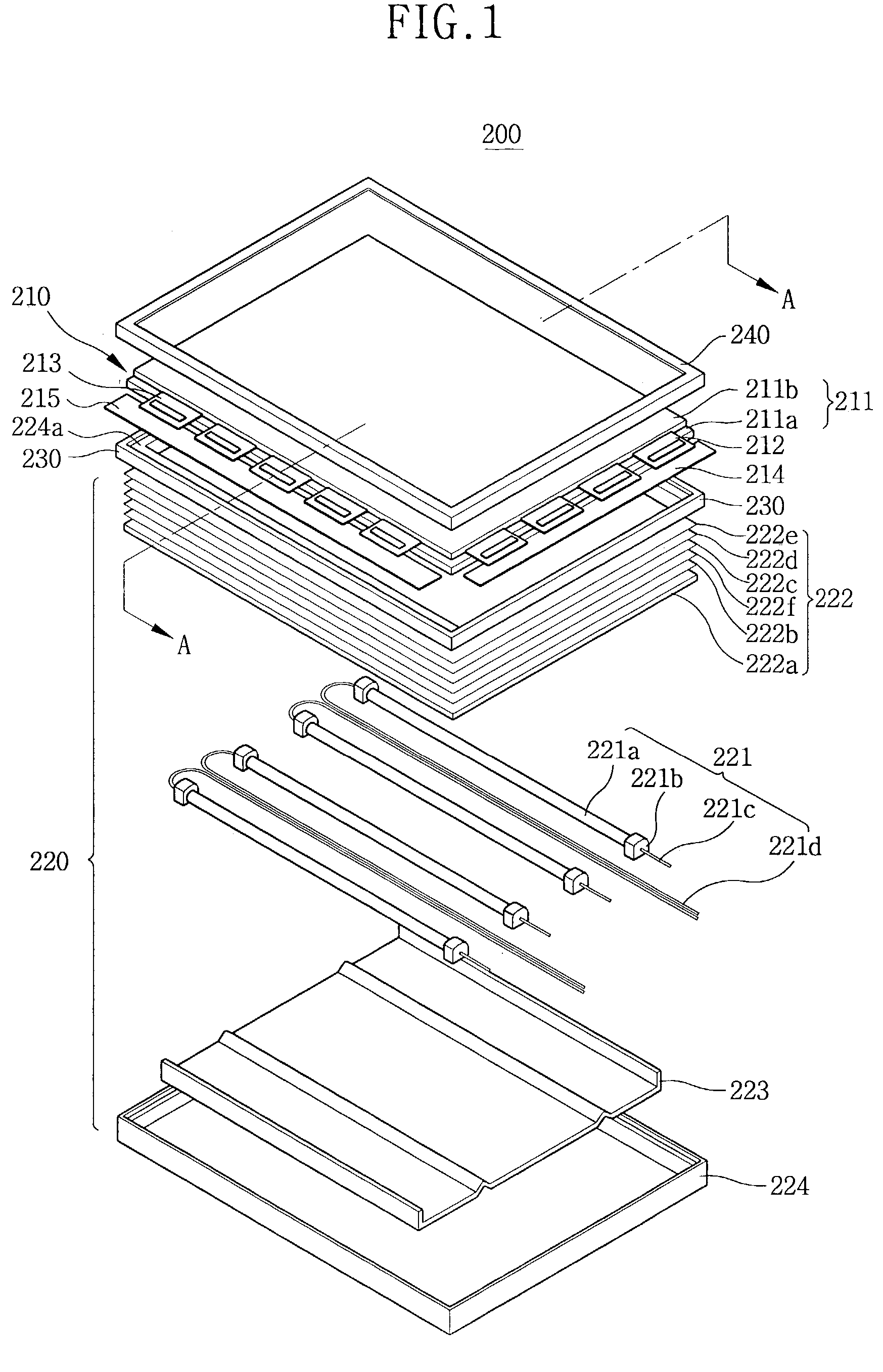
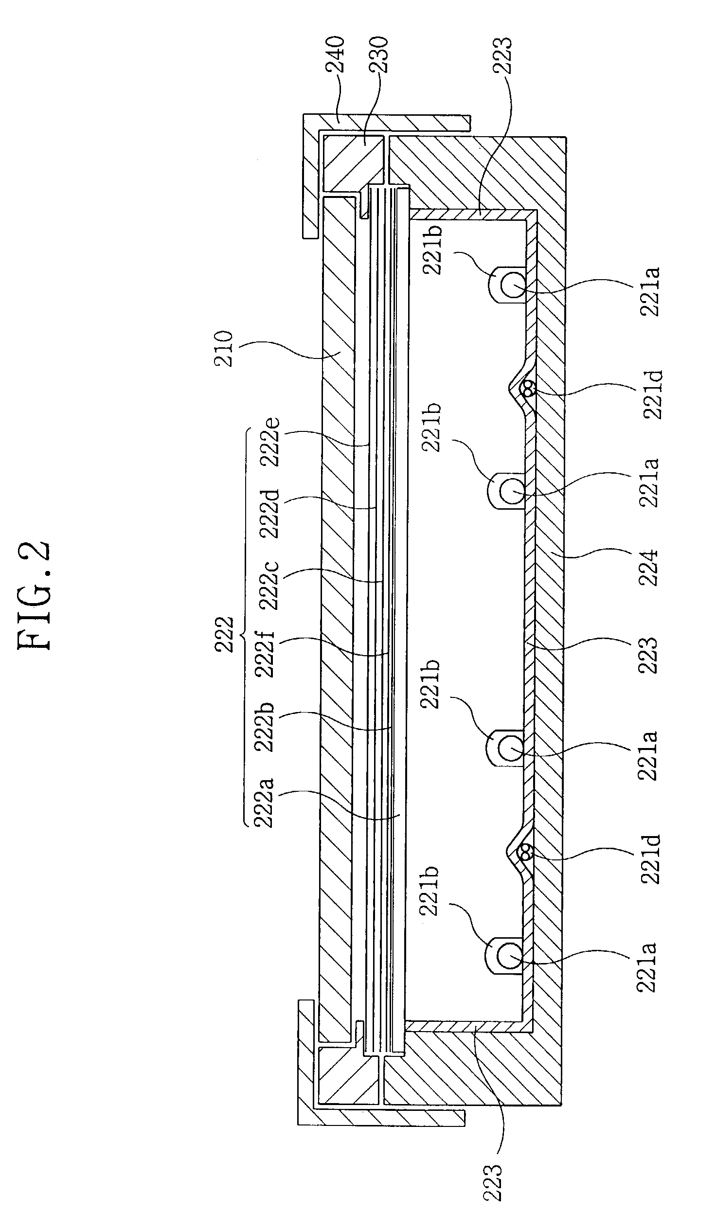
[0070]According to the backlight assembly, the noise shielding means includes a conductive material coated or deposited on the rear surface or the front surface of the diffusing sheet, so that the noise generated from the power voltage signal applied to the light source may be prevented from electrically affecting the liquid crystal display panel.

[0071]FIG. 4 is a schematic cross-sectional view showing a second modified embodiment of the backlight assembly shown in FIG. 1. The second modified backlight assembly includes a diffusing plate, and a conductive material is coated on a rear (or front) surface of the diffusing plate.

[0072]Referring to FIG. 4, the second modified backlight assembly 420 includes a light source 421 for generating light, a light-distribution changing means 422 for changing an optical distribution of the light exiting from the light source 421, and a reflecting plate 423 disposed under the light source 421.

[0073]The light source 421 includes a plurality of lamps...

second modified embodiment

[0079]According to the backlight assembly, the noise shielding means includes a conductive material coated or deposited on the rear surface or the front surface of the diffusing plate, so that the noise generated from the power voltage signal applied to the light source may be prevented from affecting the liquid crystal display panel.

[0080]FIG. 5 is a schematic cross-sectional view showing a third embodiment of the backlight assembly as shown in FIG. 1. The third modified backlight assembly includes a luminance-intensifying sheet, and a conductive material is coated on a rear surface of the luminance-intensifying sheet. FIG. 6 is a cross sectional view showing an example of the luminance-intensifying sheet shown in FIG. 5.

[0081]Referring to FIG. 5, the third modified backlight assembly 520 includes a light source 521 for generating light, a light-distribution changing means 522 for changing an optical distribution of the light exiting from the light source 521, and a reflecting plat...


PUM


Abstract

Disclosed is an LCD device including a noise shielding member. The noise shielding member is a transparent conductive member including a transparent film on which a transparent conductive layer is coated. The noise shielding member may also be a transparent conductive layer scattered on the optical sheets. The transparent conductive layer comprises ITO or IZO. The noise shielding member is disposed under the diffusing plate or interposed between optical sheets. The noise shielding member may be disposed under the LCD panel. The noise generated from the electric power signal applied to the lamp of the backlight assembly is shielded from the LCD panel. Furthermore, the noise shielding member and optical sheets contacts with the chassis of the LCD device through various ground members so as to be connected to earth potential and be electrically stabilized. Accordingly, display quality of the LCD device is improved.

Description

CROSS-REFERENCE OF RELATED APPLICATIONS[0001]This application relies for priority upon Korean Patent Application No. 2002-31085 filed on Jun. 3, 2002, Korean Patent Application No. 2002-75134 filed on Nov. 29, 2002, and Korean Patent Application No. 2002-48691 filed on Aug. 17, 2002, the contents of which are herein incorporated by reference in their entirety.BACKGROUND OF THE INVENTION[0002]1. Field of the Invention[0003]The present invention relates to a liquid crystal display device, and more particularly, to a liquid crystal display device having a noise shielding means for shielding a noise generated from a power voltage signal applied to a light source from a liquid crystal display panel of the liquid crystal display device.[0004]2. Description of the Related Art[0005]Display devices as information processing devices have various shapes and functions. The display device functions as an interfacing devices between users and the information processing devices such that the users...

Claims


Application Information

Patent Timeline
IPC IPC(8): G02F1/1333F21S2/00F21V23/00F21Y103/00G02F1/13G02F1/13357
CPCG02F1/133604G02F1/133605G02F1/133608G02F2201/46G02F2001/133334G02F2001/133612G02F2001/133317G02F1/133317G02F1/133334G02F1/133612
Inventor LEE, TAE-JINPARK, JONG-DAELEE, JEONG-HWANCHOI, YONG-SEOKHAN, BYUNG-WOONG
Owner SAMSUNG DISPLAY CO LTD
Why Eureka
Try Eureka