Method for fabricating fine features by jet-printing and surface treatment

a technology of surface treatment and jet printing, which is applied in the direction of coatings, transistors, solid-state devices, etc., can solve the problems of corresponding problems in both techniques, and high cost of large-area array fabrication

Inactive Publication Date: 2005-12-06
XEROX CORP
View PDF6 Cites 108 Cited by
  • Summary
  • Abstract
  • Description
  • Claims
  • Application Information

AI Technical Summary

Problems solved by technology

However, fabricating such large-area arrays is expensive.
A large part of the fabrication cost of the large-area arrays arises from the photolithographic process used to pattern the array.
Both techniques have corresponding problems.
Toner-based materials are hard to control and difficult to remove after deposition.
The use of ink-jetted liquids to directly write etch masks is a practical alternative to printed toner although jet printing also possesses inherent complexities.
Controlling the feature sizes of printed liquid masks is difficult due to spreading of the liquid on the surface after deposition.
However these printed droplets may adhere poorly.
Neither situation is desirable in semiconductor processing—the small contact angle droplets increase feature size while large contact angle droplets give unreliable patterning.
However, even with these printheads, the small sizes of features critical to the fabrication of large-area microelectronic arrays have been difficult to achieve.

Method used


Image

  • Method for fabricating fine features by jet-printing and surface treatment
  • Method for fabricating fine features by jet-printing and surface treatment
  • Method for fabricating fine features by jet-printing and surface treatment

Examples


Embodiment Construction

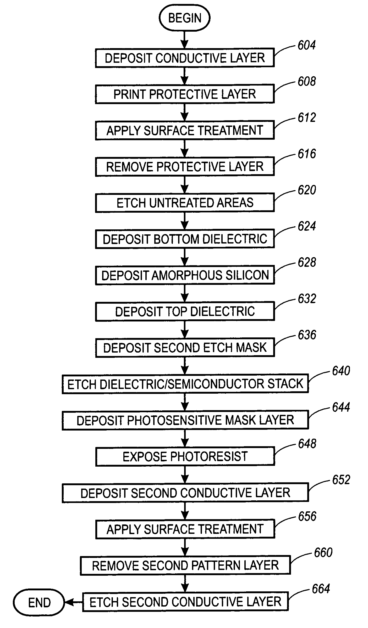
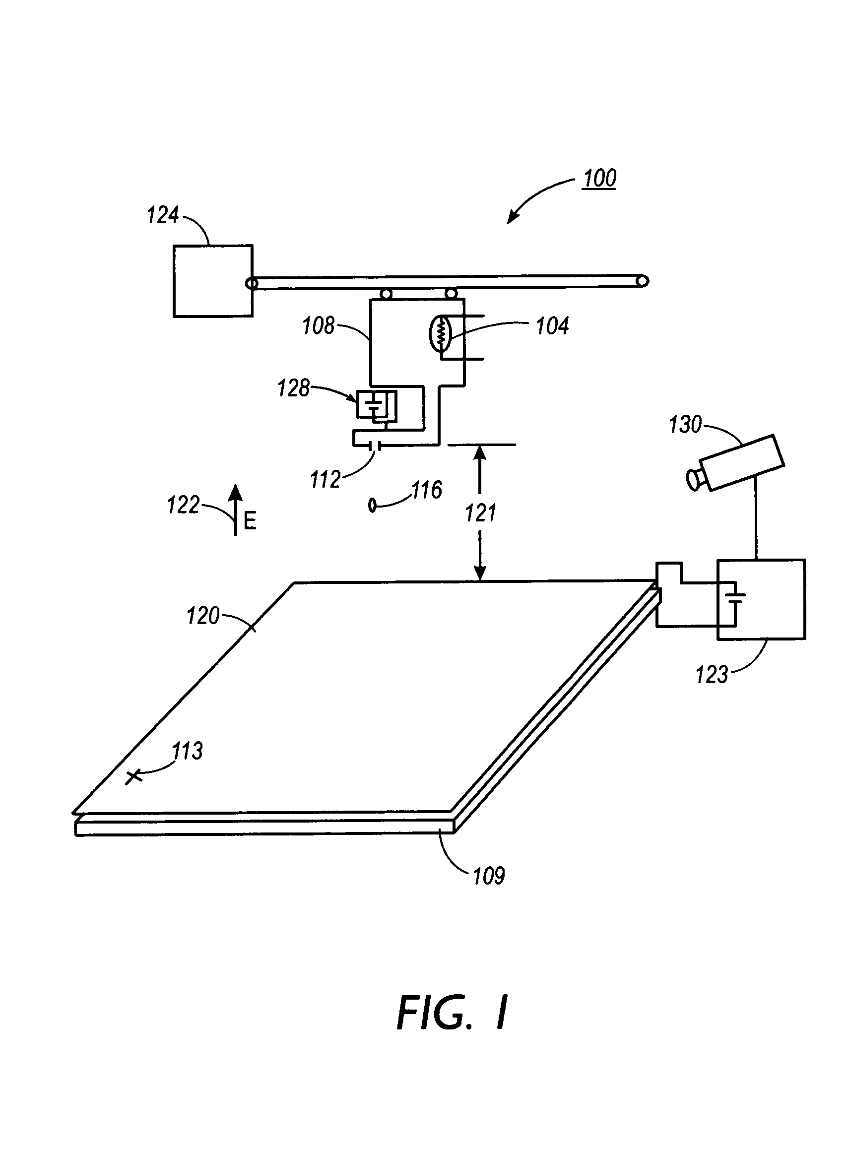
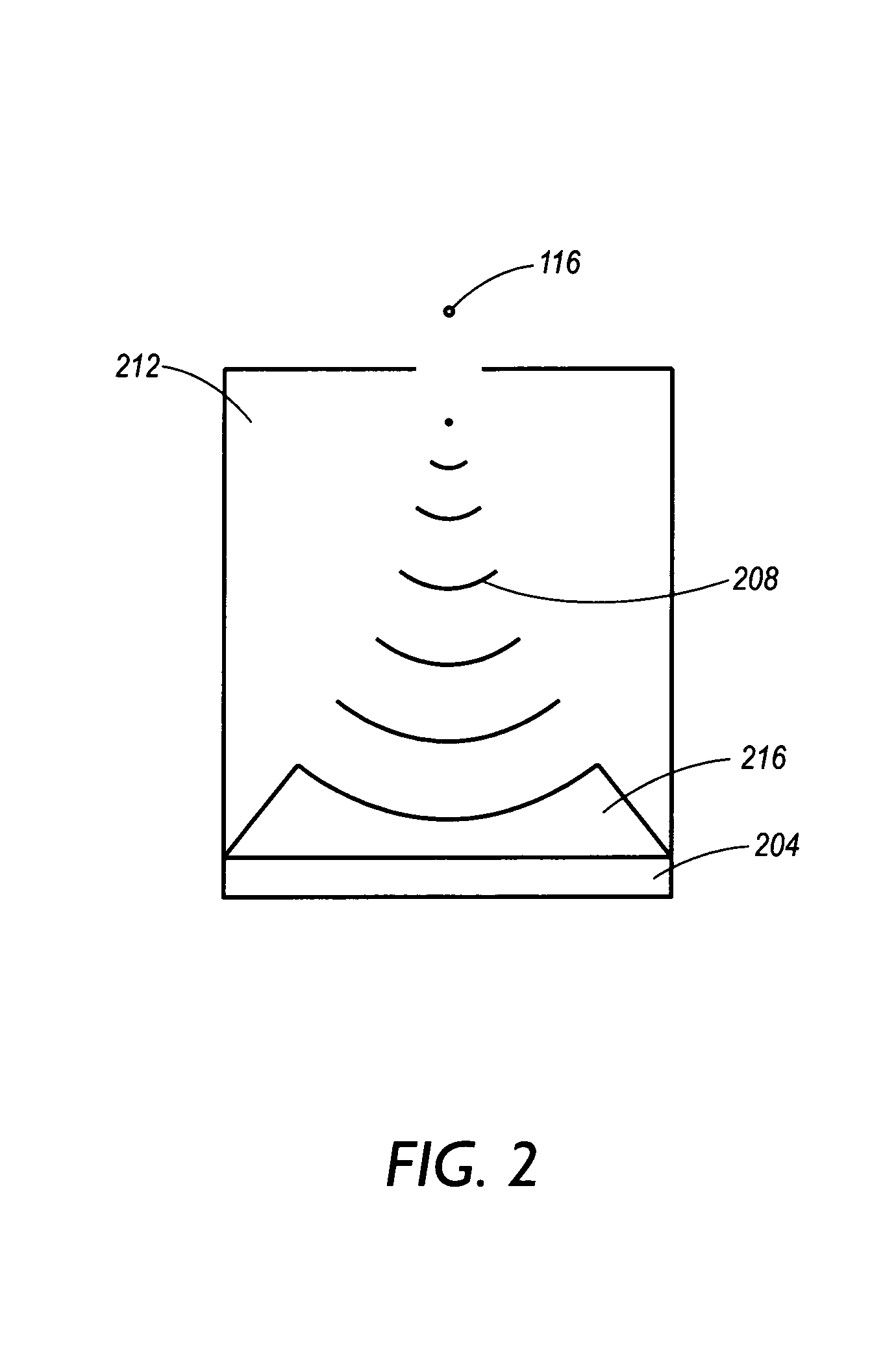
[0019]In the following detailed description a method and system of forming fine-feature devices on a substrate using printed patterns will be described. The system will create a pattern, typically using a printer to controllably eject individual droplets to form a patterned protective layer or coating over regions of the substrate to define the outline of a feature. Regions that were not at one time covered by protective layer will be subject to deposition (or removal) of materials used to form various features. Thus feature size will not be limited by droplet size, but instead by how closely droplets can be positioned together without combining to form a single droplet. A system to tightly control the boundaries of the droplet and minimize possible coalescence of juxtaposed droplets will also be described.

[0020]FIG. 1 shows a system 100 including a heat source 104 that heats a reservoir 108 of typically phase-change material to a temperature that is sufficient to maintain the mater...


PUM

PropertyMeasurementUnit
widthaaaaaaaaaa
sizesaaaaaaaaaa
feature sizeaaaaaaaaaa

Abstract

A method and system for masking a surface to be etched is described. The method includes the operation of heating a phase-change masking material and using a droplet source to eject droplets of a masking material for deposit on a thin-film or other substrate surface to be etched. The temperature of the thin-film or substrate surface is controlled such that the droplets rapidly freeze after upon contact with the thin-film or substrate surface. The thin-film or substrate is then treated to alter the surface characteristics, typically by depositing a self assembled monolayer on the surface. After deposition, the masking material is removed. A material of interest is then deposited over the substrate such that the material adheres only to regions not originally covered by the mask such that the mask acts as a negative resist. Using such techniques, feature sizes of devices smaller than the smallest droplet printed may be fabricated.

Description

BACKGROUND[0001]In recent years, the increasingly widespread use of display device alternatives to the cathode ray tube (CRT) has driven the demand for large-area electronic arrays. In particular, amorphous silicon and laser-recrystallized poly-silicon liquid crystal displays are commonly used in lap-top computers. However, fabricating such large-area arrays is expensive. A large part of the fabrication cost of the large-area arrays arises from the photolithographic process used to pattern the array. In order to avoid such photolithographic processes, direct marking techniques have been considered as an alternative to photolithography.[0002]Examples of direct marking techniques used in place of photolithography include utilizing a xerographic process to deposit a toner that acts as an etch mask and using an ink-jet printhead to deposit a liquid mask. Both techniques have corresponding problems. Toner-based materials are hard to control and difficult to remove after deposition.[0003]...

Claims


Application Information

Patent Timeline
Patent Type & Authority Patents(United States)
IPC IPC(8): B05D1/26B05D1/32B05D7/00H01L21/033H01L21/288H01L21/311H01L21/3205H01L21/3213H01L21/336H01L29/786H01L51/00H01L51/05H01L51/40
CPCB82Y30/00H01L21/0337H01L21/31144H01L21/32139H01L29/66765H01L51/0004H01L51/0021H01L51/0023H01L51/0541H10K71/13H10K71/621H10K71/60H10K10/464
Inventor WONG, WILLIAM S.READY, STEVEN E.WHITE, STEPHEN D.SALLEO, ALBERTOCHEBINYC, MICHAEL L.
Owner XEROX CORP
Why Eureka
Try Eureka