

Fabricating a tapered hole incorporating a resinous silicon containing film
a technology of resinous silicon and tapered holes, applied in the direction of gas-filled discharge tubes, semiconductor/solid-state device details, electric discharge tubes, etc., can solve the problems of poor contact, poor contact, and poor coverage of the material or ito of the pixel electrode b>312/b>, and achieve the effect of good contact, good contact, and poor conta
- Summary
- Abstract
- Description
- Claims
- Application Information
AI Technical Summary
Benefits of technology
Problems solved by technology
Method used
Image

Examples
example 1
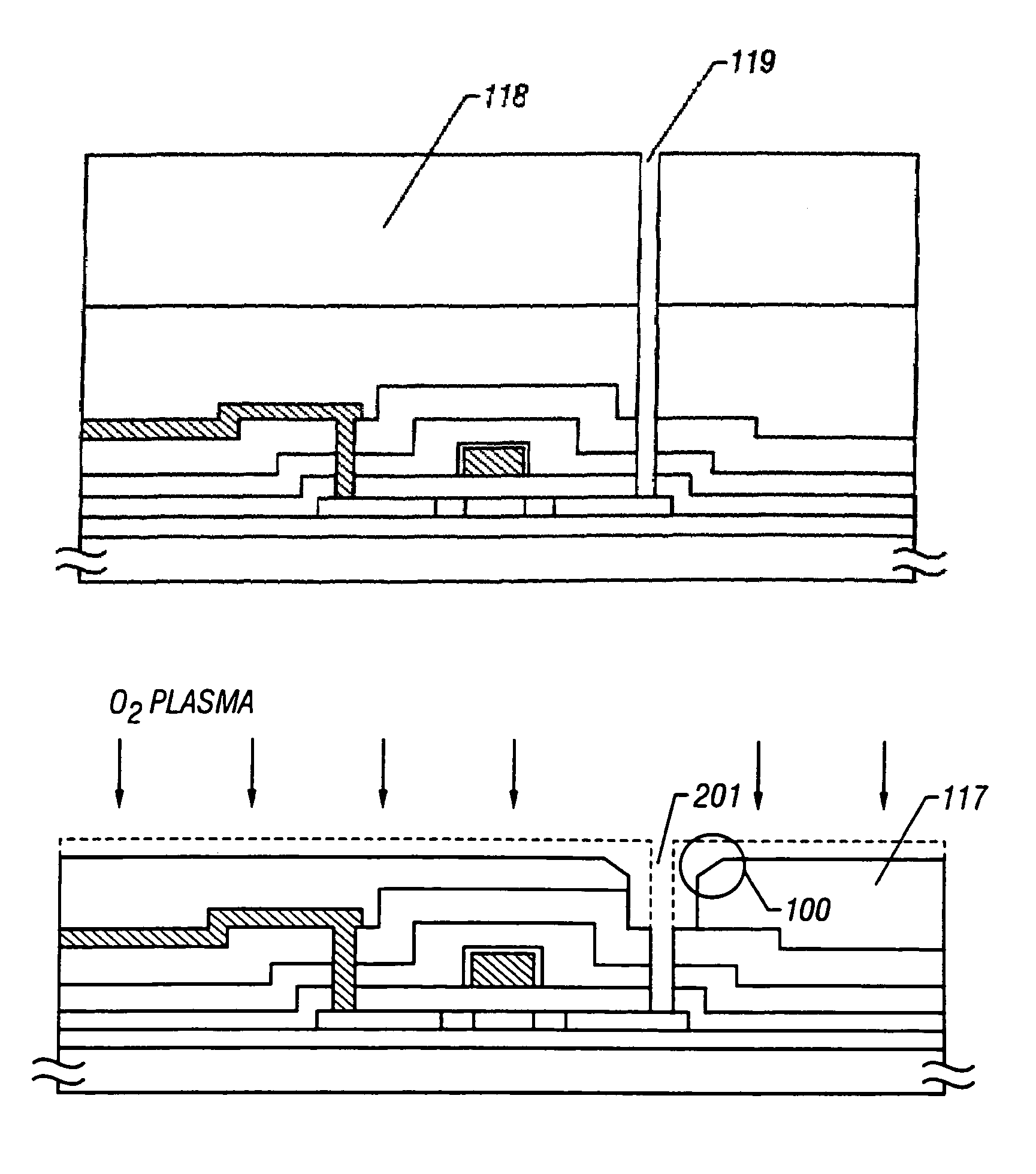
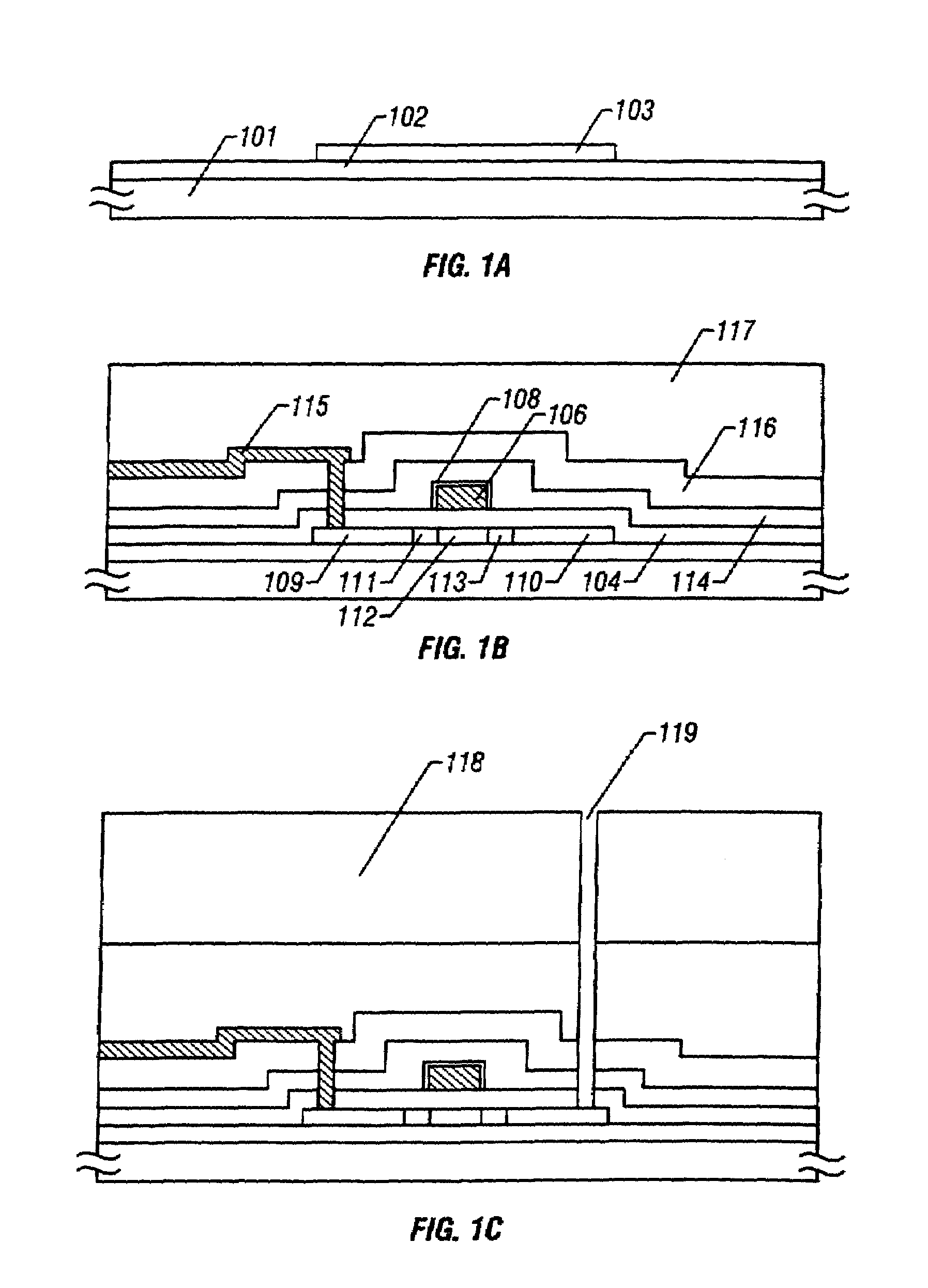
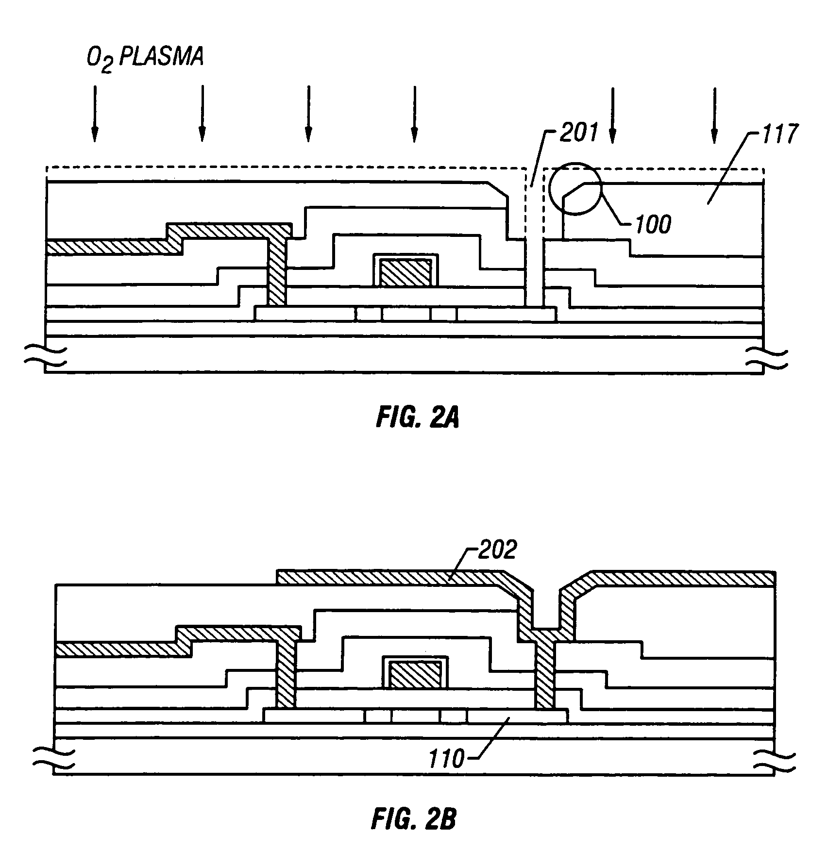
[0028]The present example pertains to steps for fabricating TFTs arranged in pixel regions of an active matrix liquid crystal display.
[0029]FIGS. 1(A)–1(C) illustrate steps for fabricating a TFT according to the present example. First, a silicon oxide film is formed as a buffer layer 102 on a substrate 101 of glass or quartz to a thickness of 3000 Å by plasma CVD. Then, an amorphous silicon film (not shown) is formed to a thickness of 500 Å by plasma CVD or LPCVD. This amorphous silicon film will become a starting film in forming the active layer of the TFT.
[0030]Then, the amorphous silicon film (not shown) is crystallized by illuminating it with laser light or heat-treating it. Thus, a crystalline silicon film is obtained. This crystalline silicon film will form the active layer of the TFT later.
[0031]Thereafter, the crystalline silicon film (not shown) is patterned to form the active layer 103 of the TFT. In this way, a state shown in FIG. 1(A) is obtained.
[0032]Then, a silicon ox...
example 2
[0050]The present example is similar to Example 1 described already except that the buffer layer 102 and the gate-insulating film 104 are both made of silicon oxynitride (SiOxNy). The state of the interface between the active layer 103 of semiconductor and the surrounding portion (i.e., the buffer layer 102 and the gate-insulating film 104) greatly affects the operation of the TFT.
[0051]Generally, a silicon oxide film or the like is used as a buffer layer. However, any special attention is not paid to the quality of the film. On the other hand, with respect to a gate-insulating film, much attention has been given to it, because it is considered that the gate-insulating film greatly affects the characteristics of the TFT.
[0052]Our findings reveal that it is necessary to pay much attention to the quality of the buffer layer underlying an active layer, as well as to the gate-insulating film, because the quality of the buffer layer materially affects the long-term reliability of the TFT...
example 3
[0055]The present example pertains to separate technical means for widening window holes formed in an interlayer dielectric film made of a resinous material.
[0056]A method of forming window holes in accordance with the present example is illustrated in FIGS. 4(A)–4(D). First, as shown in FIG. 4(A), a first interlayer dielectric film 401 is formed from silicon oxide, silicon nitride, or other silicide. A layer underlying the first dielectric film is not shown but a semiconductor layer, a metallization layer, or other dielectric layer can be formed at will under the first dielectric film.
[0057]After forming the first dielectric film 401, a second interlayer dielectric film 402 is formed from a resinous material on the first dielectric film. Then, a mask 403 of photoresist is formed on the second interlayer dielectric film 402. This resist mask 403 is provided with a window hole 404 to expose the second interlayer dielectric film 402 of the resinous material (FIG. 4(A)).
[0058]Then, the...
PUM
 Abstract
Description
Claims
Application Information