

Array substrate, display device and manufacture method of the array substrate
A technology of an array substrate and a manufacturing method, applied in the field of flat panel display, can solve the problems of poor contact between IC chips and array substrate terminals, increased short circuit of wiring, and reduced contact area, etc.
- Summary
- Abstract
- Description
- Claims
- Application Information
AI Technical Summary
Problems solved by technology
Method used
Image

Examples
Embodiment Construction
[0021] The following will clearly and completely describe the technical solutions in the embodiments of the present invention with reference to the accompanying drawings in the embodiments of the present invention. Obviously, the described embodiments are only some, not all, embodiments of the present invention. Based on the embodiments of the present invention, all other embodiments obtained by persons of ordinary skill in the art without creative efforts fall within the protection scope of the present invention.
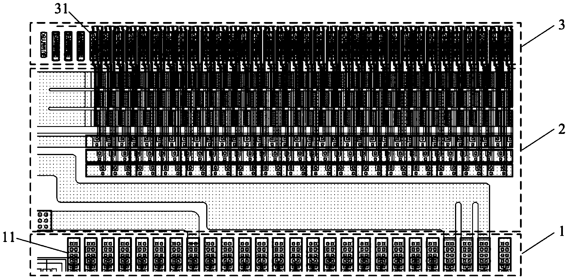
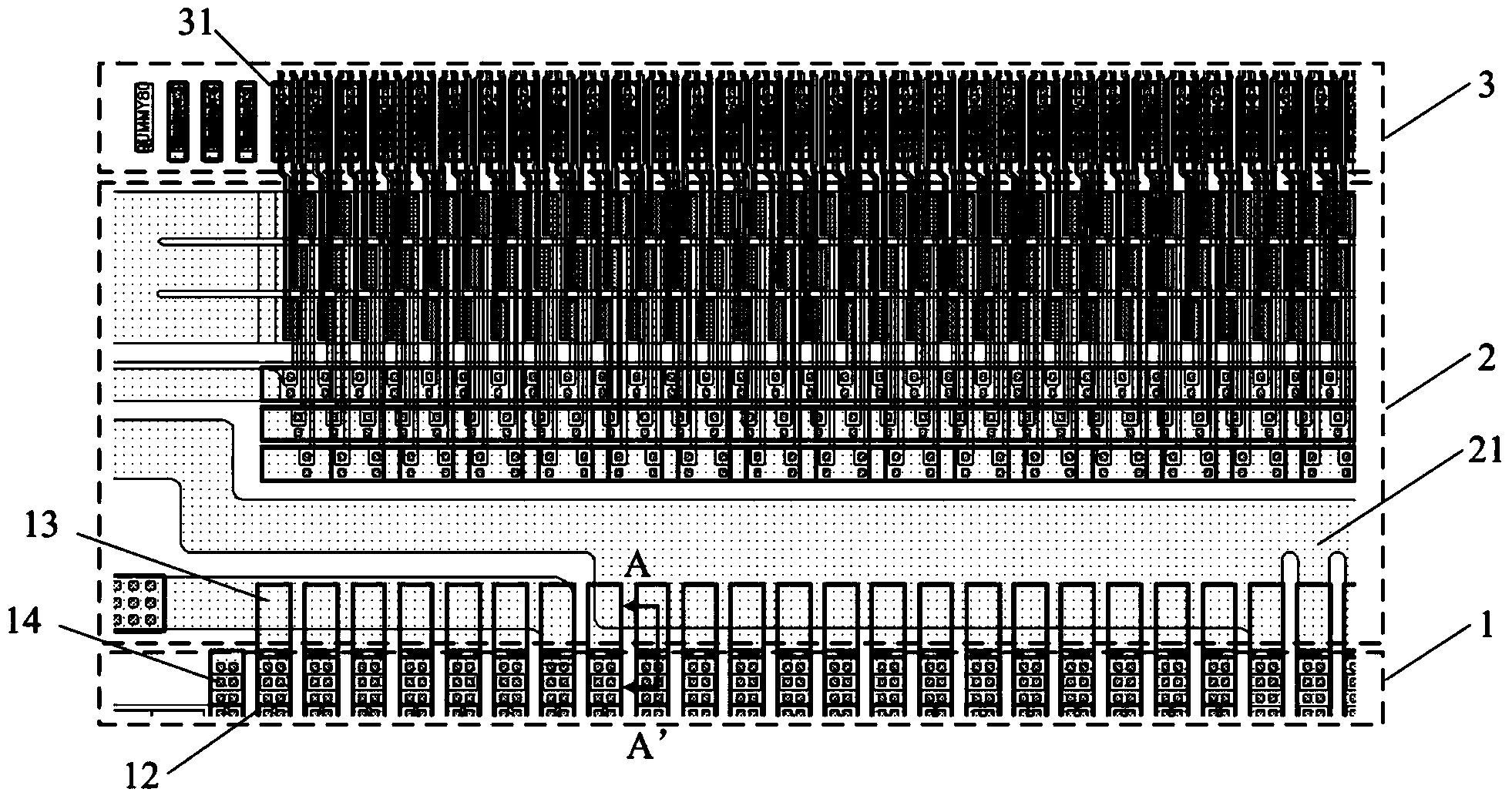
[0022] The array substrate usually includes a display area and a frame area. The display area includes a plurality of pixel units arranged in a matrix. Each pixel unit is provided with a thin film transistor switch. The screen display is realized by controlling the liquid crystal molecules in the pixel unit. The frame area surrounds the display area. The periphery of the area is used to set peripheral circuits to provide pixel unit display picture signals.
[0023]...
PUM
 Abstract
Description
Claims
Application Information