Semiconductor testing apparatus

Active Publication Date: 2015-07-16
WILLTECH
View PDF2 Cites 12 Cited by
  • Summary
  • Abstract
  • Description
  • Claims
  • Application Information

AI Technical Summary

Benefits of technology

[0015]The present invention has been proposed to solve such problems of the related art, and an object of the invention is to provide a semiconductor testing apparatus in that a testing pin is rendered to electrically connect to another testing pin or an external substrate t

Problems solved by technology

At this time, if the electrical contact between one testing pin 111 among many testing pins and the space transformer 130 is unstable, there is a problem in that the result of the DUT test becomes imprecisely.
Due to this, the reliability of the test res

Method used


Image

  • Semiconductor testing apparatus
  • Semiconductor testing apparatus
  • Semiconductor testing apparatus

Examples


Embodiment Construction

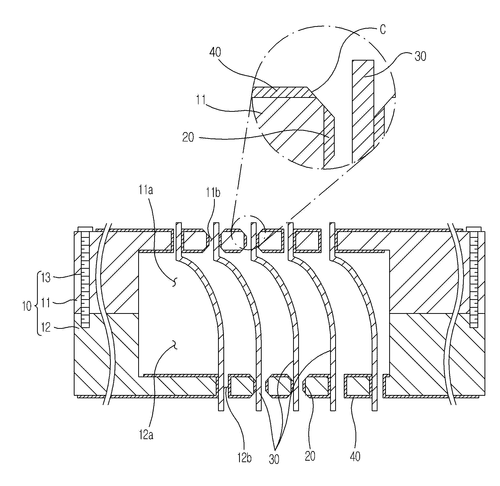
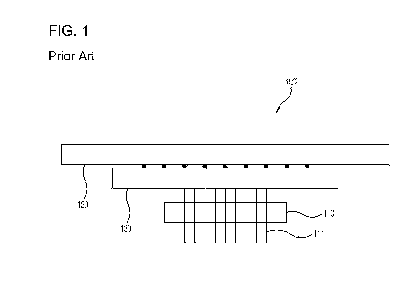
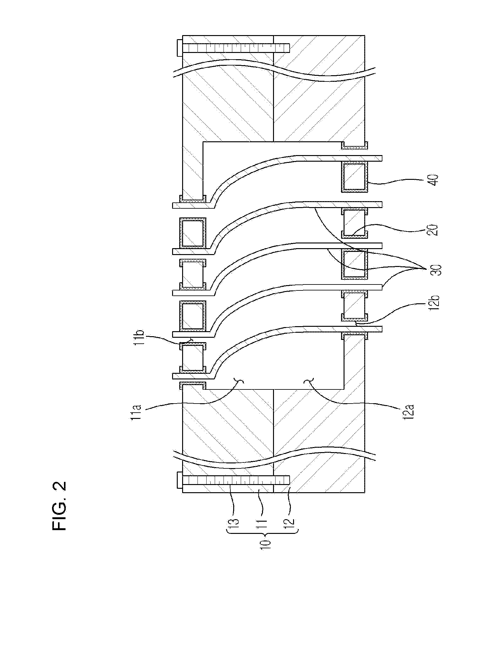
[0031]Hereinafter, a preferred embodiment of the invention will be described in detail with reference to the accompanying drawings. Hereinafter, in order to simply make the description, the probe card will be explained as the term called as a semiconductor testing apparatus. However, the present invention is not limited to the probe card. All semiconductor testing apparatus having multiple test pins can be applied thereto.

[0032]FIG. 2 is a schematic cross-sectional view showing a semiconductor testing apparatus according to one embodiment of the present invention; FIG. 3 is a conceptual diagram showing a state in that a conductive traces according to one embodiment of the present invention is connected between conductive layers, with which the testing pin of transmitting the same signal is contacted; FIG. 4 is a drawing showing a state in that a conductive trace according to one embodiment of the present invention is extended; FIG. 5a is a drawing showing an upper surface of an uppe...


PUM


Abstract

Provided is a semiconductor testing apparatus that a testing pin is rendered to electrically connect to another testing pin or an external substrate through a conductive layer formed in the guide hole, so that it results in enhancement in various characteristics such as poor electrical contact of the testing pin, space efficiency, noise, and high frequency characteristics, thereby improving reliability in testing results.

Description

CROSS REFERENCE[0001]The present application claims the benefit of Korean Patent Application No. 10-2014-0004576 filed in the Korean Intellectual Property Office on 14 Jan. 2014, the entire contents of which are incorporated herein by reference.BACKGROUND OF THE INVENTION[0002]1. Field of the Invention[0003]The present invention relates to a semiconductor testing apparatus, and more particularly, to a semiconductor testing apparatus in that a testing pin is rendered to electrically connect to another testing pin or an external substrate through a conductive layer formed in the guide hole, so that it results in enhancement in various characteristics such as poor electrical contact of the testing pin, space efficiency, noise, and high frequency characteristics, thereby improving reliability in testing results.[0004]2. Description of the Related Art[0005]A semiconductor testing process can divide into a previous process testing, which is an EDS (Electrical Die Sorting) for testing the ...

Claims


Application Information

Patent Timeline
IPC IPC(8): G01R1/067G01R31/26
CPCG01R31/2601G01R1/06733G01R1/07342G01R1/07357G01R1/07371
Inventor KIM, IL
Owner WILLTECH
Why Eureka
Try Eureka