Electron emission device, method of manufacturing the same, and image display apparatus using the same

a technology of electron emission device and manufacturing method, which is applied in the manufacture of electrode systems, discharge tubes luminescnet screens, and discharge tubes with screens, etc. it can solve the problems of large irradiated area on an irradiated surface, easy deterioration of electron convergence, and large irradiation area, so as to achieve uniform electron emission and electron convergence. , the effect of accurate electron emission layer siz

Inactive Publication Date: 2005-12-06
PANASONIC CORP
View PDF5 Cites 18 Cited by
  • Summary
  • Abstract
  • Description
  • Claims
  • Application Information

AI Technical Summary

Benefits of technology

[0029]By such methods, it is possible that the cathode electrode includes a hole penetrating through the cathode electrode, and since the substrate forms the bottom of the hole, the processing accuracy

Problems solved by technology

Electrons emitted from electron emission devices generally expand at angles in a range of several tens degrees to the orthogonal direction to the substrate; accordingly, the convergence of electrons can easily deteriorate.
However, it is considered that the conventional electron emission device described above still leaves room for improvement.
It is considered that this makes an irradiated area

Method used


Image

  • Electron emission device, method of manufacturing the same, and image display apparatus using the same
  • Electron emission device, method of manufacturing the same, and image display apparatus using the same
  • Electron emission device, method of manufacturing the same, and image display apparatus using the same

Examples


first embodiment

[First Embodiment]

[0050][Entire Construction of Image Display Apparatus]

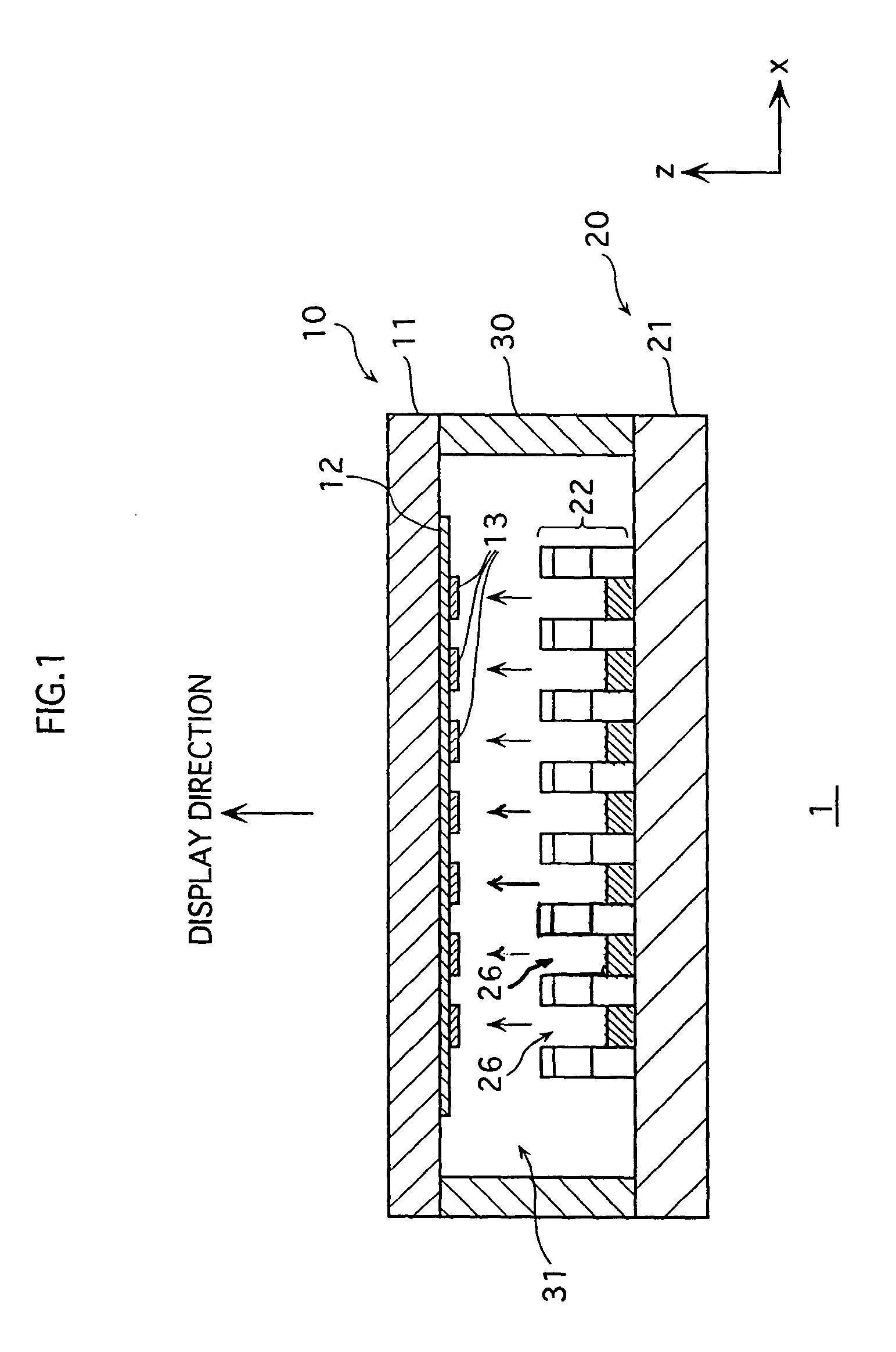
[0051]FIG. 1 is a schematic cross-sectional view of an image display apparatus 1 according to the First Embodiment. The construction of the image display apparatus 1 is explained with reference to FIG. 1.

[0052]As shown in FIG. 1, the construction of the image display apparatus 1 is such that a front panel 10 and a back panel 20 are disposed facing each other with a gap material 30 sandwiched therebetween, and space 31 between the panels is maintained in a high vacuum status.

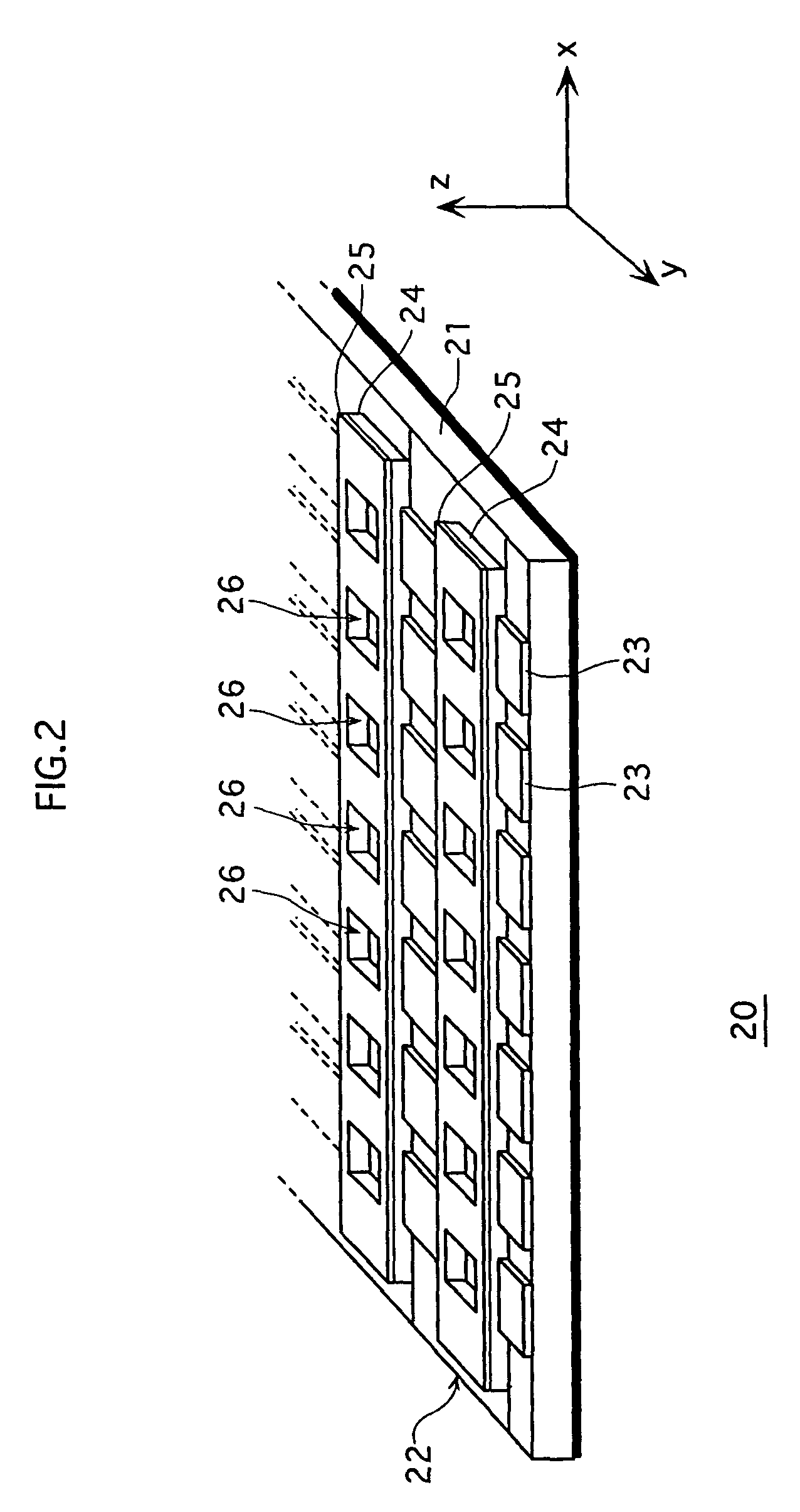
[0053]The front panel 10 comprises a front glass substrate 11, an anode electrode 12, and phosphor layers 13, the anode electrode 12 covering a rear side of the front glass substrate 11, and the phosphor layers 13 being disposed on a surface of the anode electrode 12 by pixel.

[0054]The front glass substrate 11 is a flat plate substrate made of soda glass, for example. Soda glass is excellent in smoothness, and also desirable in terms of produ...

second embodiment

[Second Embodiment]

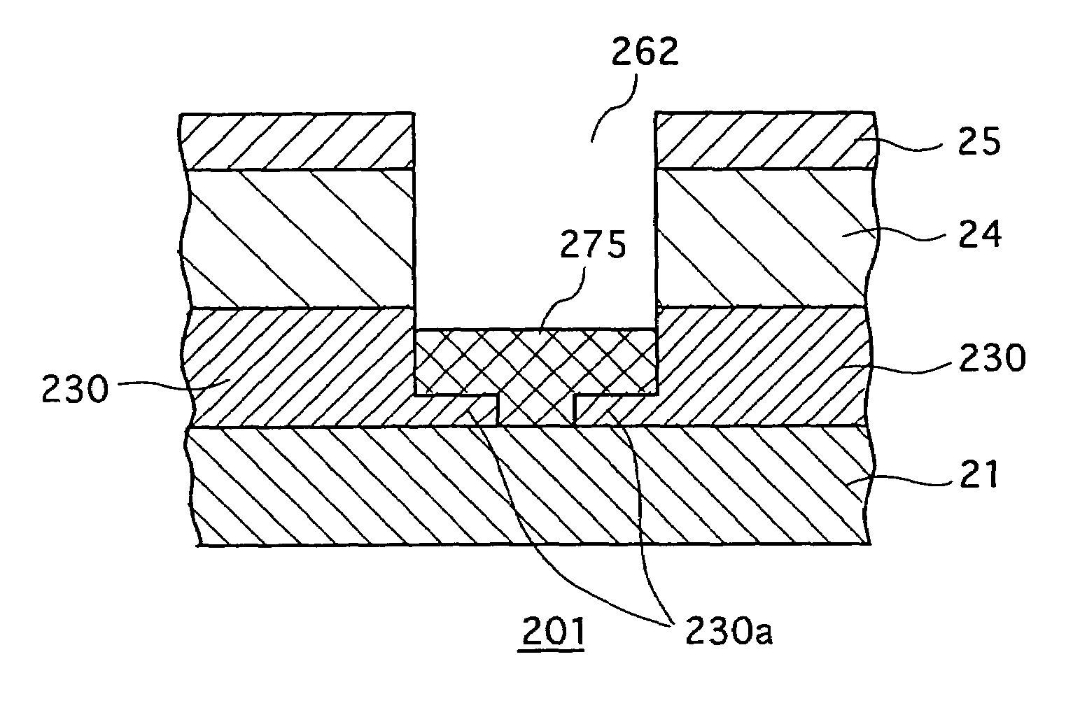
[0102]The image display apparatus according to the Second Embodiment has a similar construction with the image display apparatus described in the First Embodiment, and is only different in a shape of electron emission layers of a back panel, and therefore, explanation about the electron emission layer is mainly described below.

[0103]While, in the First Embodiment described above, the upper surface of the electron emission layer is formed almost flat, an upper surface of the electron emission layer of the Second Embodiment is concave.

[0104]FIG. 8 is a cross-sectional view of a back panel 203 according to the Second Embodiment. Note that members having the same reference numbers as in FIG. 3 are the same with the First Embodiment, and therefore detailed explanation is left out.

[0105]As shown in FIG. 8, an electron emission layer 277 having a concave upper surface (hereinafter referred to as concave lens shape), where the central area is low and the peripheral area r...

modified example

[0109]In the above Second Embodiment, the upper surface of the back glass substrate 21 in contact with the electron emission layer 277 is flat. However, the present invention is not limited to it, and the upper surface of the back glass substrate 21 can be formed in a concave lens shape.

[0110]FIG. 9 is a cross-sectional view of a back panel 204 in this modified example. Note that this modified example only differs in the shapes of the electron emission layer and the back glass substrate. Members having the same reference numbers as in FIG. 8 are the same components, and thus, detailed explanation is left out to simplify.

[0111]As shown in FIG. 9, in this modified example, the back glass substrate 210 having a concave 211 on the upper surface is in contact with an electron emission layer 278. By applying a paste containing electron emission material similar to the First Embodiment to the concave 211, the electron emission layers 278 is formed such that the electron emission layers 278...


PUM


Abstract

An object of the present invention is to provide electron emission devices having improved electron convergence.
To this end, an electron emission device of the present invention is such that a cathode electrode, an insulating layer, and a gate electrode are layered on a substrate in an order; an electron emission layer is in a first hole on the substrate penetrating from the gate electrode through the cathode electrode; an upper surface of the electron emission layer is between an upper surface of the substrate and a boundary between the cathode electrode and the insulating layer; at least one of a side surface and a lower surface except for a central area of the electron emission layer contacts the cathode electrode.
By such an electron emission device, electrons are emitted mainly from the peripheral area of the electron emission layer. Accordingly, the electron convergence is improved.

Description

TECHNICAL FIELD[0001]The present invention relates to so-called cold-cathode type (field emission type) electron emission devices, methods of manufacturing the same, and image display apparatus using the same. In particular, the present invention relates to the technique to improve convergence of electrons emitted from electron emission devices.BACKGROUND ART[0002]In recent years, image display apparatuses as thin flat panel display apparatuses have been proposed, in which minute cold-cathode type (field emission type) electron emission devices are disposed on a panel in matrix and phosphor layers are formed on a facing panel. With such a construction, images are displayed when, excited by electrons emitted from the electron emission devices to which driving voltage is applied selectively, the phosphor layers emit light.[0003]In such image display apparatuses, improving the convergence of electrons emitted from the electron emission devices has been demanded in order to support high...

Claims


Application Information

Patent Timeline
IPC IPC(8): H01J1/304H01J9/02H01J29/04H01J31/12
CPCB82Y10/00H01J1/304H01J9/025H01J31/127H01J2201/30426H01J2201/30469C01B32/05H01J9/02
Inventor SHIRATORI, TETSUYAAKIYAMA, KOJIKUROKAWA, HIDEO
Owner PANASONIC CORP
Why Eureka
Try Eureka