
Synthetic anti-parallel spin valve with thin AFM layer for very high density application

a spin valve and anti-parallel technology, applied in the field of spin valve type of gmr sensor, can solve the problems of reducing the ultimate magnetoresistive sensitivity of svmr operation, reducing exchange bias energy (jsub, hysteresis effects), and reducing shield-to-shield spacing. , the effect of thinning the stack

Inactive Publication Date: 2005-12-06
HEADWAY TECH INC
View PDF12 Cites 14 Cited by
  • Summary
  • Abstract
  • Description
  • Claims
  • Application Information

AI Technical Summary

Benefits of technology

[0009]A first object of this invention is to provide a method for forming a SVMR sensor having a thinner stack and, therefore, decreased shield-to-shield spacing.
[0012]A fourth object of this invention is to provide a method for forming a SVMR sensor having improved hysteresis properties.

Problems solved by technology

This current loss reduces the ultimate magnetoresistive sensitivity of SVMR operation because the shunted portion of the current is unaffected by resistance changes and cannot contribute to the voltage variations that are ultimately sensed.
However, thinning the AFM layer will reduce the exchange bias energy (Jex) between that layer and the pinned layer.
In addition, it is found that the AFM pinning layer produces another disadvantageous effect, it creates hysteresis effects (open R-H loops) in the relationship between R (magnetoresistance) and H (external magnetic field).
This hysteresis is due to the AFM induced anisotropy, Hck, which leads to sensor instability.
Unfortunately, when the AFM pinning layer is reduced in thickness to improve sensor resolution, the induced anisotropy is not reduced although the pinning energy is.
Therefore, the hysteresis effect becomes worse.

Method used


Image

  • Synthetic anti-parallel spin valve with thin AFM layer for very high density application
  • Synthetic anti-parallel spin valve with thin AFM layer for very high density application
  • Synthetic anti-parallel spin valve with thin AFM layer for very high density application

Examples


Embodiment Construction

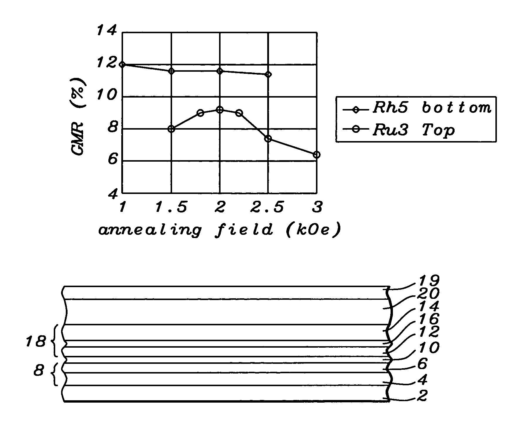
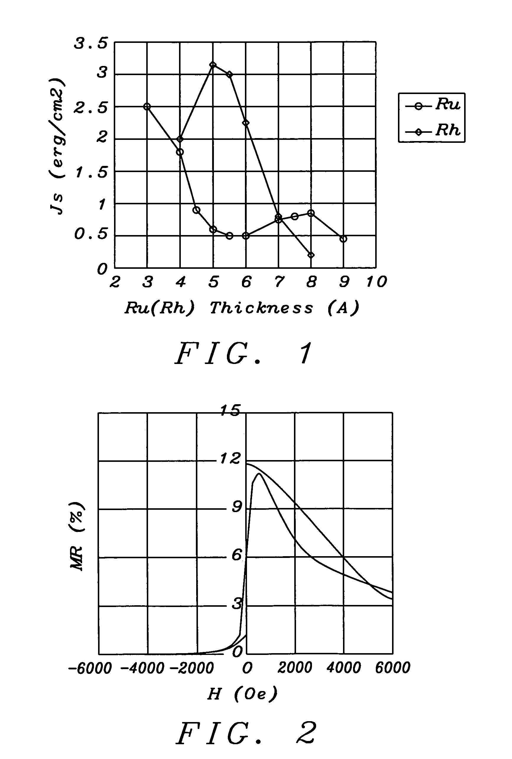
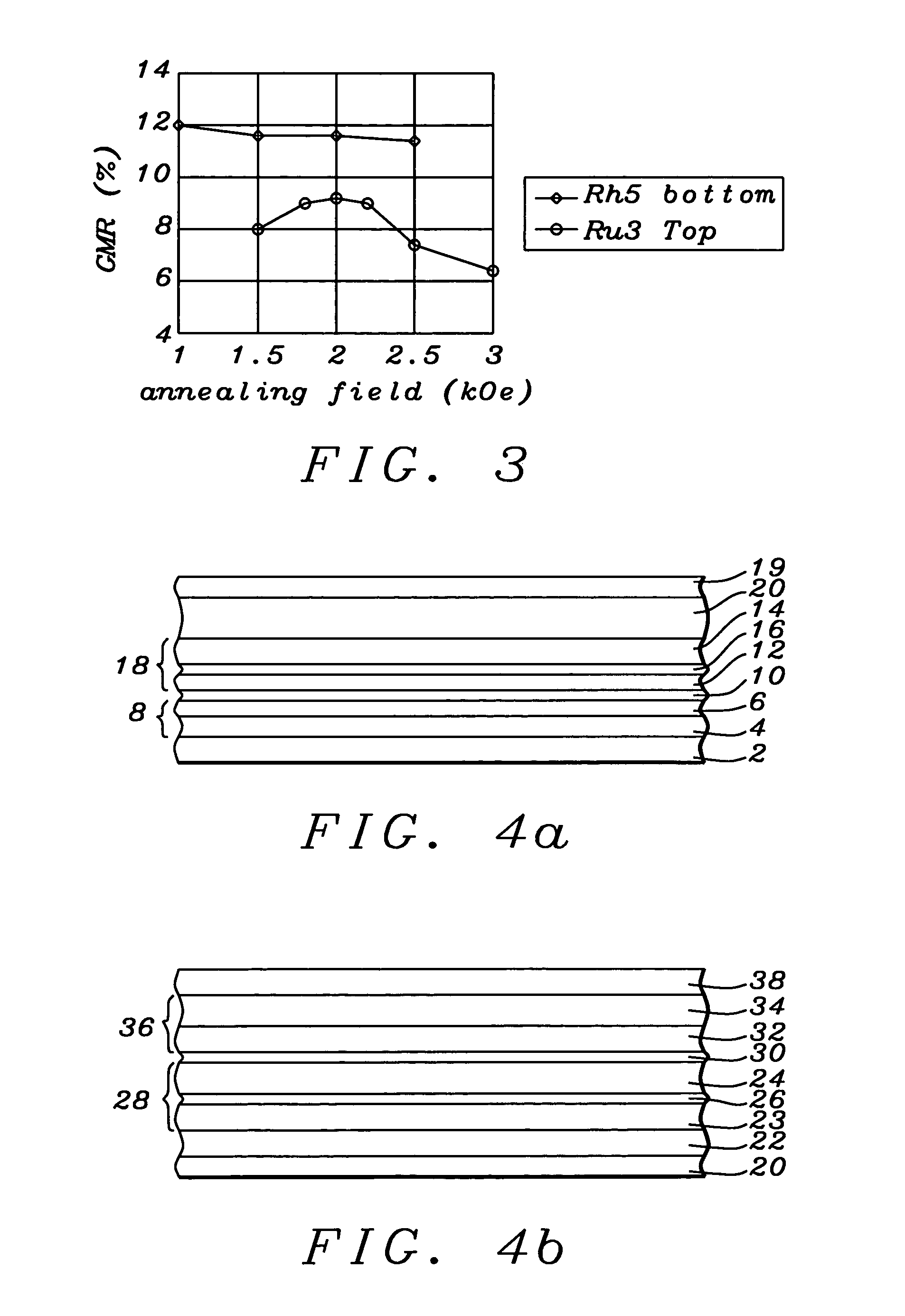
[0022]The present invention provides a method for forming both top and bottom type spin valve magnetoresistive (SVMR) read sensors having synthetic antiferromagnetically pinned (SyAP) layers (two ferromagnetic layers separated by a non-magnetic spacer layer and magnetized in mutually antiparallel directions) which are exchange coupled to a pinning layer formed of antiferromagnetic material (AFM). The novelty and advantageousness of the invention is its provision of a method for forming such a SVMR sensor with an exceptionally thin stack, which is a result of said stack having both a thin AFM pinning layer and an ultra-thin non-magnetic spacer layer separating the ferromagnetic layers in the SyAP pinned layer.

[0023]Reducing the AFM thickness, while maintaining pinning strength, has been found to be possible by improving the coupling between the two antiparallel (in magnetization) ferromagnetic layers, AP1 and AP2 through the use of ultra-thin non-magnetic spacer layers.

[0024]From sim...


PUM

PropertyMeasurementUnit
Thicknessaaaaaaaaaa

Abstract

A method for forming top and bottom spin valve sensors and the sensors so formed, the sensors having a strongly coupled SyAP pinned layer and an ultra-thin antiferromagnetic pinning layer. The two strongly coupled ferromagnetic layers comprising the SyAP pinned layer in the top valve configuration are separated by a Ru spacer layer approximately 3 angstroms thick, while the two layers in the bottom spin valve configuration are separated by a Rh spacer layer approximately 5 angstroms thick. This allows the use of an ultra thin MnPt antiferromagnetic pinning layer of thickness between approximately 80 and approximately 150 angstroms. The sensor structure produced thereby is suitable for high density applications.

Description

[0001]This is a division of application Ser. No. 09 / 953,546, filed Sep. 17, 2001, now U.S. Pat. No. 6,775,903.RELATED PATENT APPLICATION[0002]This application is related to Ser. No. 09 / 458,727, filing date Dec. 13, 1999, and to Ser. No. 09 / 769,813, filing date Jan. 26, 2001, both assigned to the same assignee as the current invention.BACKGROUND OF THE INVENTION[0003]1. Field of the Invention[0004]This invention relates generally to the fabrication of a giant magnetoresistive (GMR) magnetic field sensor in a magnetic read head, more specifically to a spin valve type of GMR sensor having a synthetic antiferromagnetically pinned (SyAP) layer.[0005]2. Description of the Related Art[0006]One of the most commonly used structural configurations of magnetic and non-magnetic layers in giant magnetoresistive (GMR) read-heads is the so-called spin-valve magnetoresistive (SVMR) structure. In the most basic version of the SVMR, two ferromagnetic layers such as CoFe or NiFe are separated by a thi...

Claims


Application Information

Patent Timeline
IPC IPC(8): G01R33/09G11B5/31G11B5/39H01F10/14H01F10/16H01F10/32H01F41/14H01L43/08H01L43/10H01L43/12
CPCB82Y10/00B82Y25/00G01R33/093G11B5/3903H01F10/3295H01F10/3268G11B5/3163G11B2005/3996Y10T29/49044Y10T29/49039Y10T29/49055Y10T29/49034Y10T29/49032
Inventor HORNG, CHENG T.JU, KOCHANCHEN, MAO-MINLI, MINTONG, RU-YINGLIAO, SIMON
Owner HEADWAY TECH INC
Learn More