Semiconductor processing methods of chemical vapor depositing SiO2 on a substrate

a technology of sio2 and semiconductors, applied in the field of semiconductor processing methods of chemical vapor depositing sio2 on a substrate, can solve the problems of unsatisfactory condition, unsatisfactory success, premature formation of undesirable intermediates, etc., and achieve the effect of reducing the formation of undesired reaction intermediates

Inactive Publication Date: 2005-12-13
MICRON TECH INC
View PDF25 Cites 117 Cited by
  • Summary
  • Abstract
  • Description
  • Claims
  • Application Information

AI Technical Summary

Problems solved by technology

One problem facing the semiconductor wafer processor is achieving adequate and conformal step coverage of deposited SiO2 into very deep and narrow contact openings or other so-called high aspect ratio topographies.
Such is an undesirable condition.
One source of inadequate conformality of SiO2 on a substrate surface is premature formation of undesirable intermediates which react to form SiO2 at higher topographical elevations on a substrate surface.
Unfortunately, great success has not been achieved due to significant degradation of deposition rates stemming from competitive absorption relative to the substrate surface as between the ethylene and the precursor.

Method used


Image

  • Semiconductor processing methods of chemical vapor depositing SiO2 on a substrate
  • Semiconductor processing methods of chemical vapor depositing SiO2 on a substrate
  • Semiconductor processing methods of chemical vapor depositing SiO2 on a substrate

Examples


Embodiment Construction

[0021]This disclosure of the invention is submitted in furtherance of the constitutional purposes of the U.S. Patent Laws “to promote the progress of science and useful arts” (Article 1, Section 8).

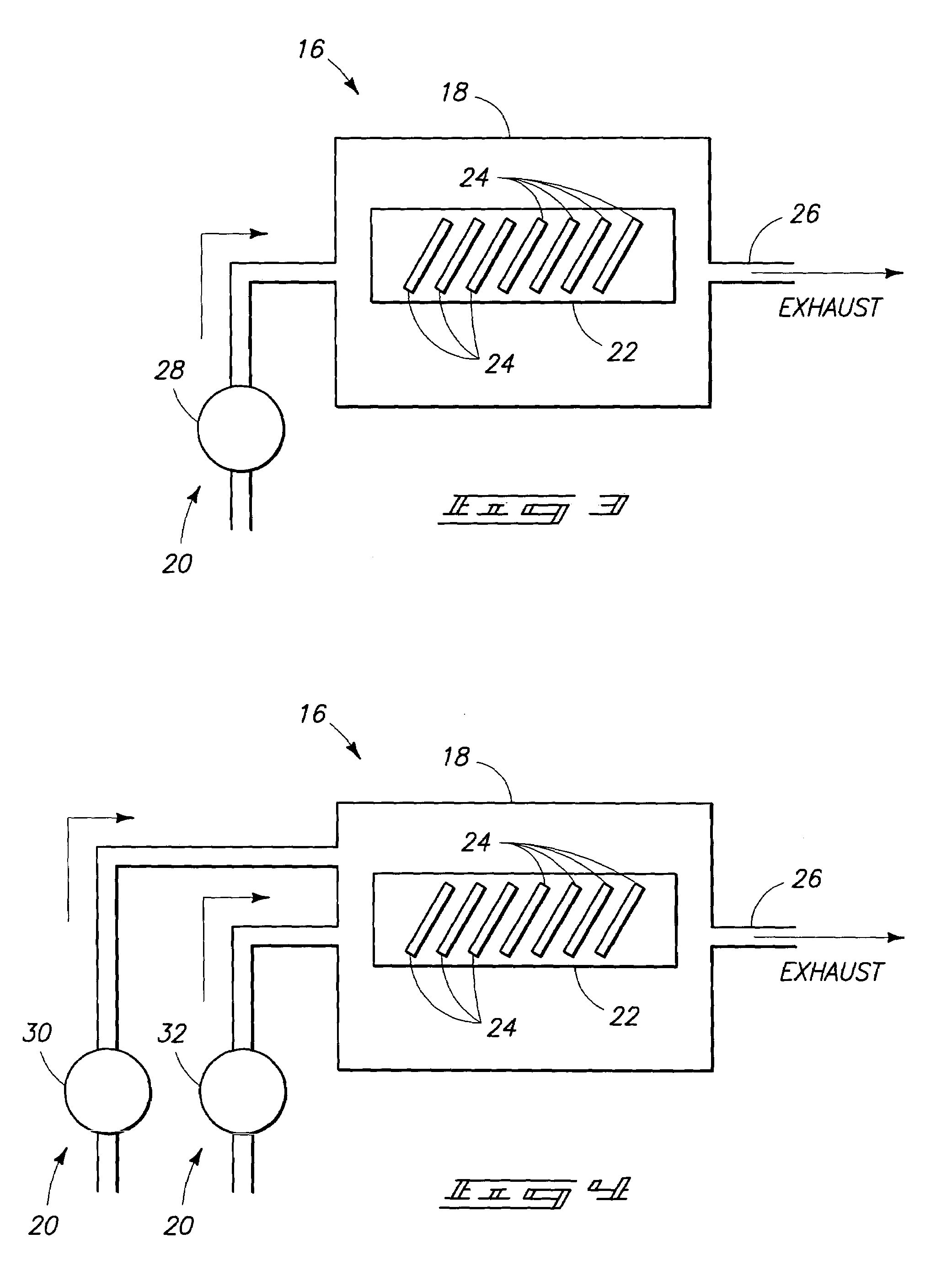
[0022]In accordance with one aspect of the invention, a semiconductor processing method of chemical vapor depositing SiO2 on a substrate comprises:

[0023]placing a substrate within a chemical vapor deposition reactor;

[0024]feeding an organic silicon precursor into the chemical vapor deposition reactor having the substrate positioned therein under conditions effective to decompose the precursor into SiO2 which deposits on the substrate and into a gaseous oxide of hydrogen; and

[0025]feeding an additional quantity of the gaseous oxide of hydrogen into the reactor while feeding the organic silicon precursor to the reactor.

[0026]In accordance with another aspect of the invention, a semiconductor processing method of reducing the decomposition rate of an organic silicon precursor in a chemical v...


PUM

PropertyMeasurementUnit
temperatureaaaaaaaaaa
internal pressureaaaaaaaaaa
temperaturesaaaaaaaaaa

Abstract

The invention provides semiconductor processing methods of depositing SiO2 on a substrate. In a preferred aspect, the invention provides methods of reducing the formation of undesired reaction intermediates in a chemical vapor deposition (CVD) decomposition reaction. In one implementation, the method is performed by feeding at least one of H2O and H2O2 into a reactor with an organic silicon precursor. For example, in one exemplary implementation, such components are, in gaseous form, fed separately into the reactor. In another exemplary implementation, such components are combined in liquid form prior to introduction into the reactor, and thereafter rendered into a gaseous form for provision into the reactor. The invention can be practiced with or in both hot wall and cold wall CVD systems.

Description

RELATED PATENT DATA[0001]This patent resulted from a divisional application of U.S. patent application Ser. No. 09 / 212,726, filed Dec. 15, 1998, which resulted from a continuation application of U.S. patent application Ser. No. 08 / 696,243 which was filed on Aug. 13, 1996 U.S. Pat. No. 5,849,644.TECHNICAL FIELD[0002]This invention relates to semiconductor processing methods of chemical vapor depositing SiO2 on a substrate.BACKGROUND OF THE INVENTION[0003]Chemical vapor deposited (CVD) SiO2 films and their binary and ternary silicates find wide use in VLSI processing. These materials find use as insulators between polysilicon and metal layers, between metal layers in multilevel metal systems, as diffusion sources, as diffusion and implantation masks, as capping layers to prevent outdiffusion, and as final passivation layers.[0004]The manner in which a thin film covers or conforms to the underlying features on a substrate is an important characteristic in semiconductor processing. Conf...

Claims


Application Information

Patent Timeline
Patent Type & Authority Patents(United States)
IPC IPC(8): C23C16/40H01L21/316
CPCC23C16/402C23C16/4411H01L21/02164H01L21/02271H01L21/31612
Inventor SCHUEGRAF, KLAUS F.
Owner MICRON TECH INC
Why Eureka
Try Eureka